Package structure and manufacturing method thereof

A technology of packaging structure and manufacturing method, which is applied in semiconductor/solid-state device manufacturing, semiconductor/solid-state device parts, instruments, etc., can solve the problems that the surface of the sensing area 110 is easy to be damaged, shorten the service life of the fingerprint image sensor, etc., so as to avoid Effects of Electronic Component Failure

Active Publication Date: 2017-06-09
SILICONWARE PRECISION IND CO LTD
View PDF6 Cites 0 Cited by
  • Summary
  • Abstract
  • Description
  • Claims
  • Application Information

AI Technical Summary

Problems solved by technology

[0007] However, the silicon crystal fingerprint image sensor needs to directly touch the sensing area 110 of the sensing chip 11 with a finger, so the surface of the sensing area 110 is easily damaged, thus shortening the service life of the existing fingerprint image sensor

Method used


Image

  • Package structure and manufacturing method thereof
  • Package structure and manufacturing method thereof
  • Package structure and manufacturing method thereof

Examples


Embodiment Construction

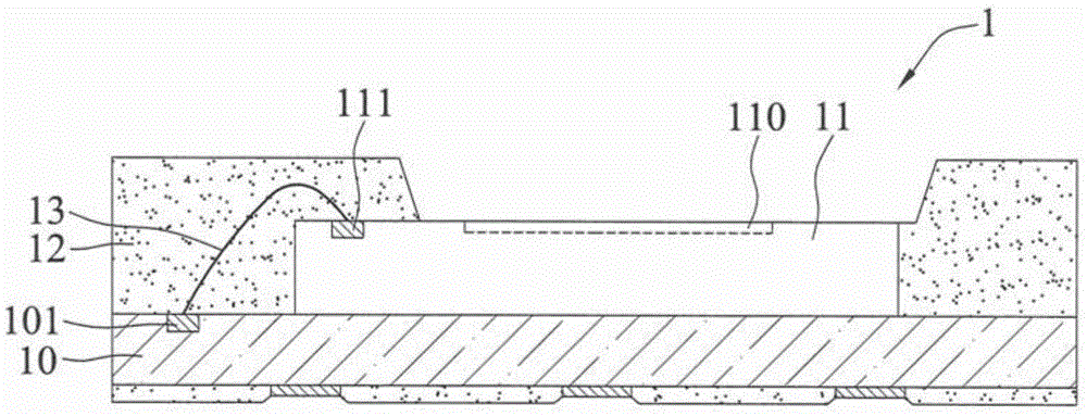
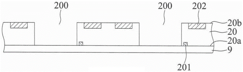
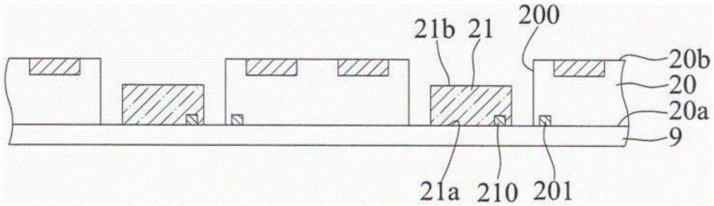
[0040] Embodiments of the present invention are described below through specific examples, and those skilled in the art can easily understand other advantages and effects of the present invention from the content disclosed in this specification. The present invention can also be implemented or applied through other different specific examples, and various modifications and changes can be made to the details in this specification based on different viewpoints and applications without departing from the spirit of the present invention.

[0041] It should be noted that the structures, proportions, sizes, etc. shown in the drawings attached to this specification are only used to match the content disclosed in the specification for the understanding and reading of those skilled in the art, and are not used to limit the implementation of the present invention. condition, so it has no technical substantive meaning, and any modification of structure, change of proportional relationship...


PUM


Abstract

A package structure and a manufacturing method thereof are disclosed. The package structure comprises a substrate, an electronic assembly, which is embedded in the substrate and has a sensing surface, and an insulating layer, which is formed on the substrate and the sensing surface. By covering the sensing surface of the electronic assembly by the insulating layer, the finger will not directly touch the sensing area, the sensing area is protected, and the failure of the electronic assembly is avoided.

Description

technical field [0001] The invention relates to a packaging structure, in particular to a packaging structure of a fingerprint sensor and a manufacturing method thereof. Background technique [0002] With the improvement of living standards, consumers pay more and more attention to privacy. Many high-end electronic products will be equipped with identification systems to increase the security of data in electronic products. Therefore, the development and design of identification systems are also following consumers. Demand has become the direction of electronics industry development. [0003] Today's identification system is mainly developed towards a biometric system. In the biometric identification system, according to different identification targets, it can be divided into two types of biometric identification systems that identify biological characteristics (such as fingerprints, pupils, faces, and voiceprints) and behavioral characteristics (such as signatures and voi...

Claims


Application Information

Patent Timeline
IPC IPC(8): G06K9/00H01L23/31H01L21/56
CPCH01L21/56H01L23/3128G06V40/1306G06V40/1329H01L2224/92H01L2224/97H01L2224/48091H01L2924/00014
Inventor 唐绍祖蔡岳颖蔡瀛洲
Owner SILICONWARE PRECISION IND CO LTD
Why Eureka
Try Eureka