Printed circuit board manufacturing method, printed circuit board and mobile terminal
A technology of printed circuit boards and metal sheets, which is applied in the field of electronics and can solve problems such as circuit breakage in the board
- Summary
- Abstract
- Description
- Claims
- Application Information
AI Technical Summary
Problems solved by technology
Method used
Image

Examples
no. 1 example
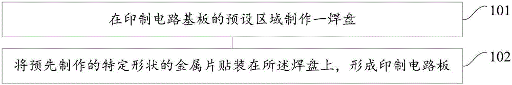
[0032] refer to Figure 1A , which shows one of the flowcharts of a method for manufacturing a printed circuit board according to the first embodiment of the present invention, which may specifically include the following steps:
[0033] Step 101, making a pad in a predetermined area of the printed circuit board;
[0034] A printed circuit board (PCB) is a support for electronic components and a carrier for electrical connections of electronic components. Almost all electronic equipment includes printed circuit boards.
[0035] In the embodiment of the present invention, the printed circuit board can be applied to a mobile terminal, and the mobile terminal can be an electronic device such as a mobile phone or a tablet computer, or an electronic device such as a smart watch or a smart bracelet. The embodiment of the present invention does not limit the specific type of the mobile terminal.
[0036] In the embodiment of the present invention, when fabricating a printed circu...
no. 2 example
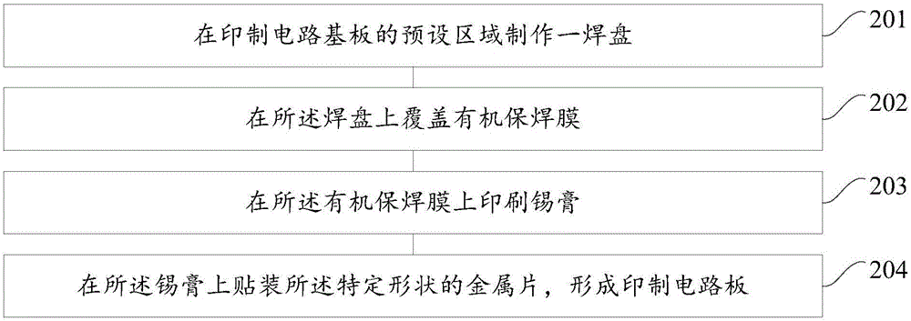
[0060] refer to figure 2 , which shows a flow chart of a method for manufacturing a printed circuit board according to the second embodiment of the present invention. The printed circuit board is applied to a mobile terminal, and may specifically include the following steps:
[0061] Step 201, making a pad in a predetermined area of the printed circuit board;
[0062] In the embodiment of the present invention, when fabricating a printed circuit board applied to a mobile terminal, a pad may be firstly fabricated on a predetermined area of the printed circuit substrate. The printed circuit board substrate may refer to a semi-finished PCB board that has not completed the production process of all printed circuit boards, and the preset area may refer to an area of weak strength or stress concentration in the printed circuit board, for example, it may be It is an area that is often impacted by external force when it is mounted on a mobile terminal such as a mobile phone. ...
no. 3 example
[0081] refer to Figure 4 , shows a cross-sectional view of a printed circuit board according to a third embodiment of the present invention, and the printed circuit board 400 may specifically include:
[0082] printed circuit board substrate 401;
[0083] A pad 402 fabricated in a predetermined area of the printed circuit board substrate 401;
[0084] A metal sheet 403 of a specific shape is mounted on the pad 402;
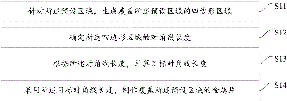
[0085] In a specific implementation, the preset area may refer to an area of weak strength or concentrated stress in the printed circuit board, for example, an area that is often impacted by external force when assembled on a mobile terminal such as a mobile phone. Further, the pads made in the preset area can have a suitable shape corresponding to the preset area. For example, the shape of the pads can be based on the range of the stress concentration area simulated by the simulation software and the space around the printed circuit board. The specific si...
PUM
 Abstract
Description
Claims
Application Information
 - Generate Ideas
- Intellectual Property
- Life Sciences
- Materials
- Tech Scout
- Unparalleled Data Quality
- Higher Quality Content
- 60% Fewer Hallucinations
Browse by: Latest US Patents, China's latest patents, Technical Efficacy Thesaurus, Application Domain, Technology Topic, Popular Technical Reports.
© 2025 PatSnap. All rights reserved.Legal|Privacy policy|Modern Slavery Act Transparency Statement|Sitemap|About US| Contact US: help@patsnap.com