TSV Reliability Analysis Method

An analysis method, the technology of through-silicon vias, applied in the field of microelectronics, can solve problems such as no consideration of stress, large storage resources, and long simulation time of electrothermal three-field coupling, etc., and achieve a wide range of applications

Active Publication Date: 2019-10-25
西安电子科技大学重庆集成电路创新研究院
View PDF3 Cites 0 Cited by
  • Summary
  • Abstract
  • Description
  • Claims
  • Application Information

AI Technical Summary

Problems solved by technology

However, 3D-TSV technology is not yet fully mature, and reliability issues have become the main obstacle to the development of TSV technology
Most researchers build finite element models of TSVs through software to analyze the reliability of TSVs. However, the situation of TSVs in actual 3D integrated circuits is very complicated. Using multi-field coupling model analysis is inefficient and requires storage resources. Especially for the reliability analysis of through-silicon vias in large-scale 3D integrated circuits, the multi-field coupling model has a low degree of convergence, which is basically impossible to achieve, and cannot accurately guide the design optimization of 3D integrated circuits
[0003] "Study on coupling analysis of electromagnetic-thermal-structure for TSV"., Nanjing, 210003, China, this paper discloses a thermodynamic analysis method of through-silicon vias coupled with three fields of electrothermal force. The article uses a finite element model, starting from The basic physical equations of each field are deduced to construct the model, which has three deficiencies: first, the model is too idealized, and does not consider the situation of through-silicon holes in the actual three-dimensional integrated circuit; The simulation time is long and the storage resources required are large; third, the model only analyzes the stress of the TSV under Gaussian pulses, and does not consider the stress around the TSV under different external excitations.

Method used


Image

  • TSV Reliability Analysis Method
  • TSV Reliability Analysis Method
  • TSV Reliability Analysis Method

Examples


Embodiment Construction

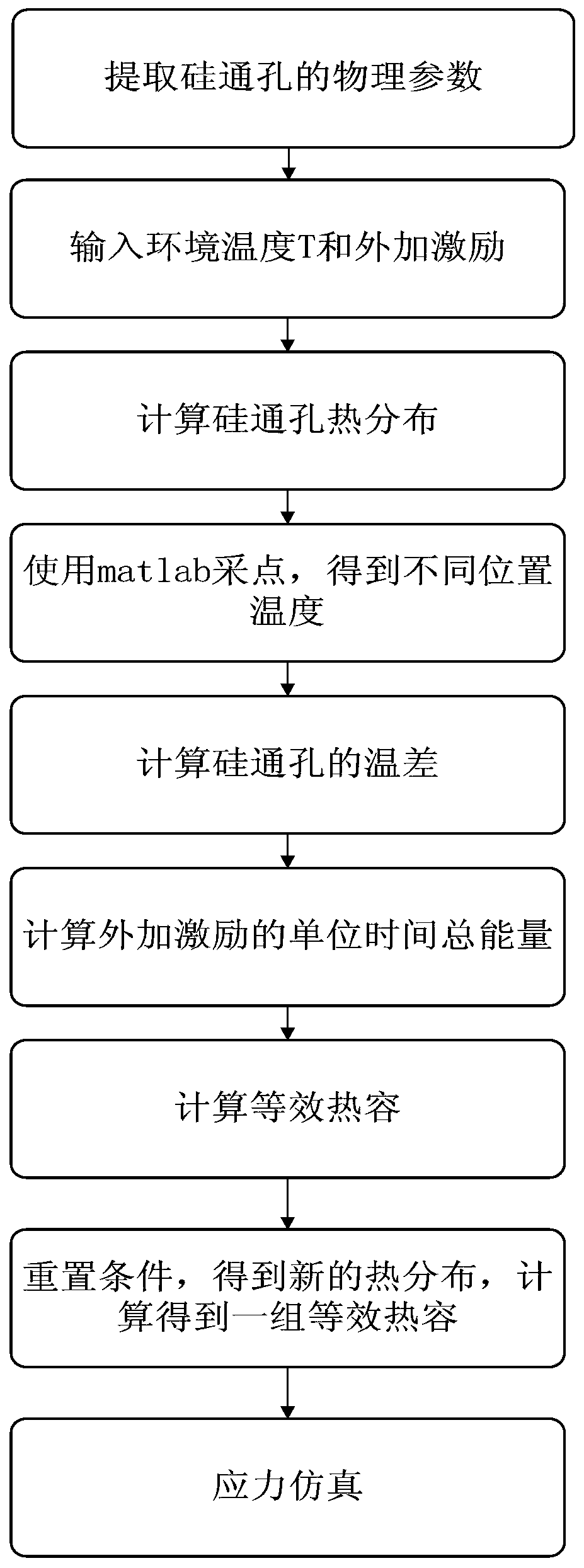
[0040] refer to figure 1 , the concrete realization of the present invention is as follows:

[0041] Step 1. Extract the physical parameters of the materials inside and outside the TSVs in the circuit.

[0042] Extract the physical parameters of the inner and outer layers of the TSV used in the circuit, the physical parameters include: the radius r of the upper surface of the TSV Cu1 , the lower surface radius r of the TSV Cu2 , the height H of the TSV, the resistance R of the copper pillar of the TSV, and the angle θ between the side surface and the bottom surface of the TSV 1 , r Cu1 Equal to the radius of the upper surface of the TSV copper pillar plus the thickness of the silicon dioxide on the upper surface of the TSV, r Cu2 It is equal to the radius of the lower surface of the TSV copper pillar plus the thickness of silicon dioxide on the lower surface of the TSV.

[0043] Step 2. Enter the ambient temperature T and external excitation used in the TSV.

[0044] Ent...


PUM


Abstract

The invention discloses a silicon through hole reliability analyzing method and aims at mainly solving the problems of long simulation time and large consumption and storage in the prior art. According to the technical scheme, the silicon through hole reliability analyzing method has the advantages that 1, physical parameters of all layers of materials inside and the outside a silicon through hole are extracted; 2, environment temperature T and extrinsic motivation of the silicon through hole are input; 3, the heat distribution of the silicon through hole is calculated by using the parameters in the steps 1 and 2; 4, point sampling is conducted on the heat distribution of the silicon through hole by adopting Matlab to obtain temperatures at different positions of the silicon through hole; 5, according to the temperatures at the different positions of the silicon through hole, the average temperature difference (shown in the description) of the silicon through hole is calculated, and the total heat Q within unit time is calculated; 7, an equivalent heat capacity value is obtained according to the temperature difference and the total energy Q; 8, new silicon through hole heat distribution is obtained by changing conditions, and a group of equivalent heat capacity values is obtained by repeating the steps 3-7; 9, stress simulation is performed by utilizing the equivalent heat capacity values in the step 7 and 8. The simulation time is shortened, the storage amount is decreased, and the silicon through hole reliability analyzing method can be used for three-dimensional integrated circuit design optimization of a silicon through hole.

Description

technical field [0001] The invention belongs to the technical field of microelectronics, and in particular relates to a method for analyzing the reliability of through-silicon holes, which can be used for design optimization of three-dimensional integrated circuits. Background technique [0002] Through-silicon via TSV technology is a key technology for the semiconductor integrated circuit industry to enter the 3D era. However, 3D-TSV technology is not yet fully mature, and reliability issues have become the main obstacle to the development of TSV technology. Most researchers build finite element models of TSVs through software to analyze the reliability of TSVs. However, the situation of TSVs in actual 3D integrated circuits is very complicated. Using multi-field coupling model analysis is inefficient and requires storage resources. Especially for the reliability analysis of through-silicon vias in large-scale 3D integrated circuits, the multi-field coupling model has low ...

Claims


Application Information

Patent Timeline
Patent Type & Authority Patents(China)
IPC IPC(8): G06F17/50
CPCG06F30/23
Inventor 董刚何映婷杨银堂
Owner 西安电子科技大学重庆集成电路创新研究院
Why Eureka
Try Eureka