Electrical interfaces and intelligent clothing
A technology of electrical interface and electrical connection, which is applied in the field of smart wearables and can solve problems such as the inability to miniaturize electronic devices
- Summary
- Abstract
- Description
- Claims
- Application Information
AI Technical Summary
Problems solved by technology
Method used
Image
Examples
Embodiment 1
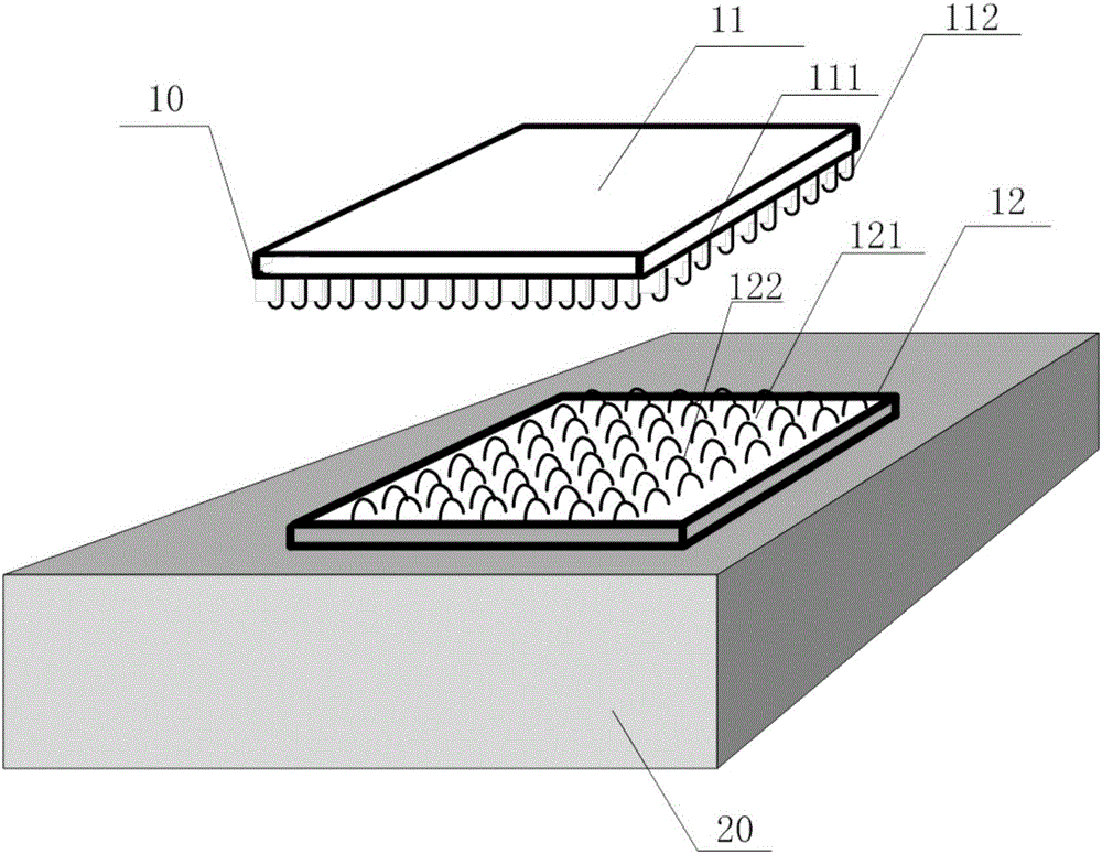
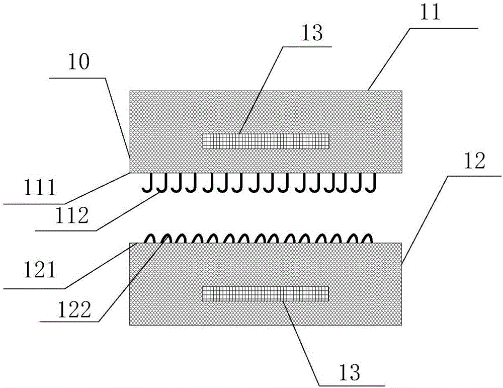
[0038] figure 1 A schematic structural diagram of an inductive electrical interface 10 provided in Embodiment 1 of the present invention, as shown in figure 1 As shown, the electrical interface 10 is used for electrical connection between the electronic device 20 and peripheral circuits, the electrical interface 10 is located outside the electronic device 20 , and specifically includes a joint 11 and an interface 12 that are separable from each other.
[0039] During use, as a possible implementation, the connector 11 can be fixed to the electronic device 20, and at the same time, the interface 12 can be fixed to the peripheral circuit; as another possible implementation, the interface 12 can be fixed to the The electronic device 20 is fixed, and at the same time, the connection between the connector 11 and the peripheral circuit is fixed.
[0040] figure 1 The fixed connection between the electronic device 20 and the interface 12 shown in the figure only shows one of the af...
Embodiment 2
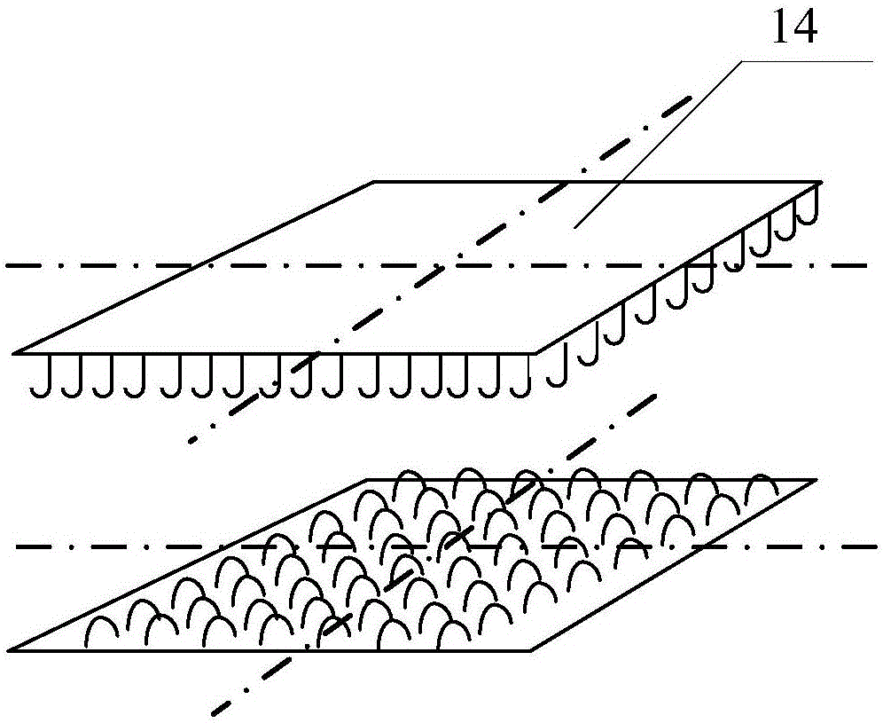
[0049] The electrical interface 10 can realize not only single-channel data or energy transmission, but also multi-channel data or energy transmission. The rough surface 121 of the interface 12 and the hook surface 111 of the joint 11 can be respectively divided into various induction areas 14, The sensing area 14 transmits a corresponding path through the sensing circuit 13 provided in the area.
[0050] image 3 A schematic diagram of the division of a sensing area 14 provided by Embodiment 2 of the present invention, as shown in image 3 As shown, on the basis of the previous embodiment, specifically, in the electrical interface 10 , the rough surface 121 of the interface 12 and the hook surface 111 of the joint 11 can be respectively divided into at least one sensing area 14 .
[0051] Specifically, a sensing circuit 13 for transmitting a path corresponding to the sensing area 14 may be provided in each sensing area 14, so as to realize multi-channel or single-channel tra...
Embodiment 3
[0062] In the aforementioned embodiments, the electrical interface 10 uses a non-contact induction method to realize electrical connection. In this embodiment, an electrical interface 40 is provided, and the interface 42 of the electrical interface 40 and the joint 41 can be connected by a hook 412 and a ring. The shape structure 422 is hooked to realize contact electrical connection.
[0063] Figure 6 A schematic structural diagram of an electrical interface 40 provided in Embodiment 3 of the present invention, as shown in Figure 6 As shown, the electrical interface 40 is used for the electrical connection between the electronic device 20 and the peripheral circuit. The electrical interface 40 is located outside the electronic device 20 and includes: a connector 41 and an interface 42 .
[0064] During use, as a possible implementation, the joint 41 can be fixed with the electronic device 20, and at the same time, the interface 42 can be fixed with the peripheral circuit; ...
PUM
 Abstract
Description
Claims
Application Information
 - Generate Ideas
- Intellectual Property
- Life Sciences
- Materials
- Tech Scout
- Unparalleled Data Quality
- Higher Quality Content
- 60% Fewer Hallucinations
Browse by: Latest US Patents, China's latest patents, Technical Efficacy Thesaurus, Application Domain, Technology Topic, Popular Technical Reports.
© 2025 PatSnap. All rights reserved.Legal|Privacy policy|Modern Slavery Act Transparency Statement|Sitemap|About US| Contact US: help@patsnap.com


