A device for carrying warped wafers and its carrying method

A wafer and warping technology, which is applied in the field of wafer carrying devices for cold plate units in the semiconductor industry, can solve problems such as easy slippage, and achieve the effects of rapid response, simple and practical carrying method, and simple device structure

Active Publication Date: 2019-03-15
SHENYANG KINGSEMI CO LTD
View PDF3 Cites 0 Cited by
  • Summary
  • Abstract
  • Description
  • Claims
  • Application Information

AI Technical Summary

Problems solved by technology

The device for carrying warped wafers can stably carry warped wafers, which solves the problem that the traditional cold plate unit carries warped wafers and is easy to slide during the lifting and lowering process of the thimble

Method used


Image

  • A device for carrying warped wafers and its carrying method
  • A device for carrying warped wafers and its carrying method
  • A device for carrying warped wafers and its carrying method

Examples


Embodiment Construction

[0020] The present invention will be described in further detail below in conjunction with the accompanying drawings.

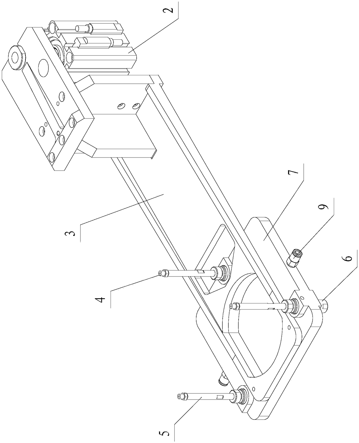
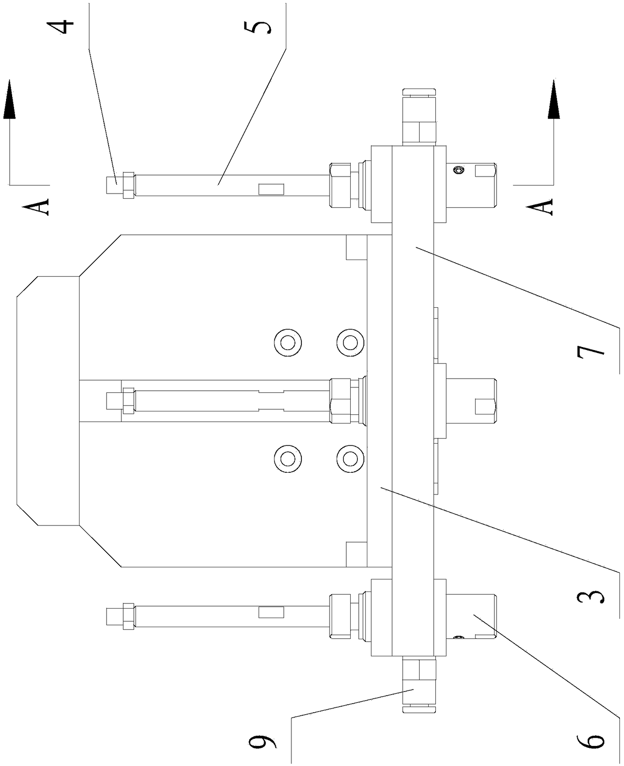
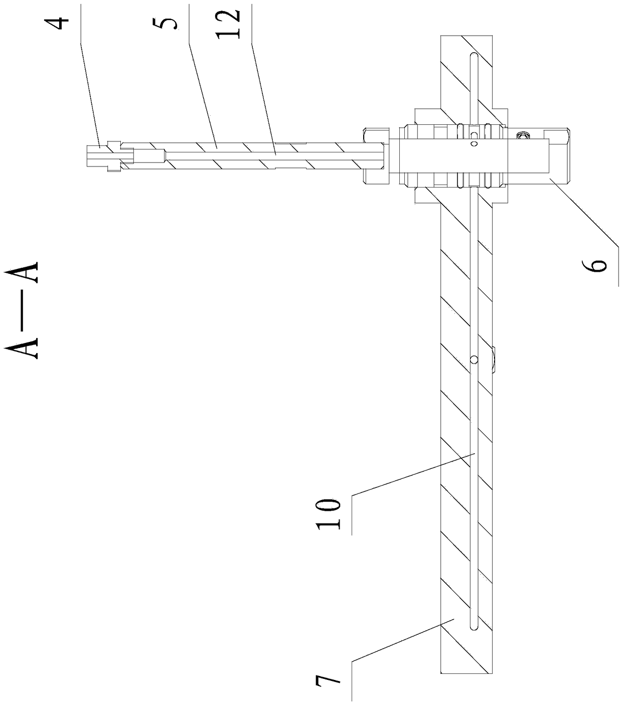
[0021] Such as Figure 1~4 As shown, the device for carrying warped wafers of the present invention includes a cylinder 2, a connecting arm 3, a suction cup 4, a thimble 5, a buffer 6 and a buffer mounting plate 7, wherein one end of the connecting arm 3 is connected to the output end of the cylinder 2, The air cylinder 2 drives the lift, and a buffer mounting plate 7 is connected under the other end of the connecting arm 3 . The buffer mounting plate 7 is provided with at least three buffers 6, and each buffer 6 is equipped with a thimble 5 with a through hole 12 inside, and the top of each thimble 5 is connected with a suction cup 4 respectively. There are three buffers 6 in this embodiment, which are arranged in a triangle on the buffer mounting plate 7; That is three) connecting holes 11, and a buffer 6 is installed in each connecting hole 11. A vacuum...


PUM


Abstract

The invention relates to a cold plate unit wafer bearing device in the semiconductor industry, in particular to a device for bearing a warped wafer and a bearing method of the device. The device comprises an air cylinder, a connecting arm, suction cups, thimbles, buffers and a buffer installation plate, wherein one end of the connecting arm is connected with an output end of the air cylinder and is driven by the air cylinder to rise and fall and the other end of the connecting arm is connected with the buffer installation plate; the buffer installation plate is provided with at least three buffers; each buffer is provided with the corresponding thimble with a through hole therein; the top ends of the thimbles are connected with the corresponding suction cups for adsorbing the warped wafer respectively; vacuum connection openings are formed in the buffer installation plate; the vacuum connection openings communicate with the buffers through a vacuum flow path arranged in the buffer installation plate, and communicate with the suction cups through the through holes in the thimbles respectively; and the suction cups are always in contact with the warped wafer through the buffers and the warped wafer is adsorbed through vacuum from the vacuum connection openings. The device plays adsorbing and grabbing roles on the warped wafer; and the warped wafer does no easily slip.

Description

technical field [0001] The invention relates to a wafer carrying device for a cold plate unit in the semiconductor industry, in particular to a device for carrying warped wafers and a carrying method thereof. Background technique [0002] Due to the deformation of the warped wafer itself, the traditional way of carrying the warped wafer on the cold plate unit cannot ensure that all three thimbles are in contact with the wafer; Easy slide. Contents of the invention [0003] The object of the present invention is to provide a device for carrying warped wafers and a carrying method thereof. The device for carrying the warped wafer can stably carry the warped wafer, and solves the problem that the traditional cold plate unit carries the warped wafer and is easy to slide when the thimble is lifted and lowered. [0004] The purpose of the present invention is achieved through the following technical solutions: [0005] The device for carrying warped wafers of the present inve...

Claims


Application Information

Patent Timeline
Patent Type & Authority Patents(China)
IPC IPC(8): H01L21/687H01L21/683
CPCH01L21/6838H01L21/68742
Inventor 李晓飞魏猛
Owner SHENYANG KINGSEMI CO LTD
Why Eureka
Try Eureka