Method and system for detecting surface defects of sip module and surface defects of exposed copper

A detection mode and module technology, applied in the direction of optical testing flaws/defects, etc., can solve the problems that the detection technology cannot meet the process standards, etc., and achieve the effect of improving the detection rate of exposed copper, reducing the misjudgment rate, and improving the recall rate

Active Publication Date: 2019-09-24
UNIVERSAL SCIENTIFIC INDUSTRIAL (SHANGHAI) CO LTD +1
View PDF7 Cites 0 Cited by
  • Summary
  • Abstract
  • Description
  • Claims
  • Application Information

AI Technical Summary

Problems solved by technology

[0004] In the prior art, a detection system equipped with a 5M Pixel black and white camera module, a Schneider lens, Pixel Size: 14um, FOV (the area actually captured by the camera): 28x35mm, and a multi-angle 6Channel composite square green light source is mainly aimed at Specific defects on the surface of the SIP module, such as copper leakage, blackening, pollution, etc., are detected for different types of defects, but the existing detection technology cannot meet the process standards, especially surface defects of exposed copper, copper leakage (exposed copper) detected by the machine Surface defect misjudgment rate reaches about 40%

Method used


Image

  • Method and system for detecting surface defects of sip module and surface defects of exposed copper
  • Method and system for detecting surface defects of sip module and surface defects of exposed copper
  • Method and system for detecting surface defects of sip module and surface defects of exposed copper

Examples


Embodiment Construction

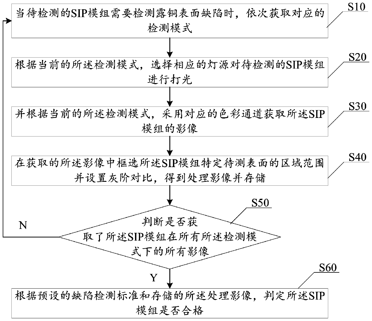
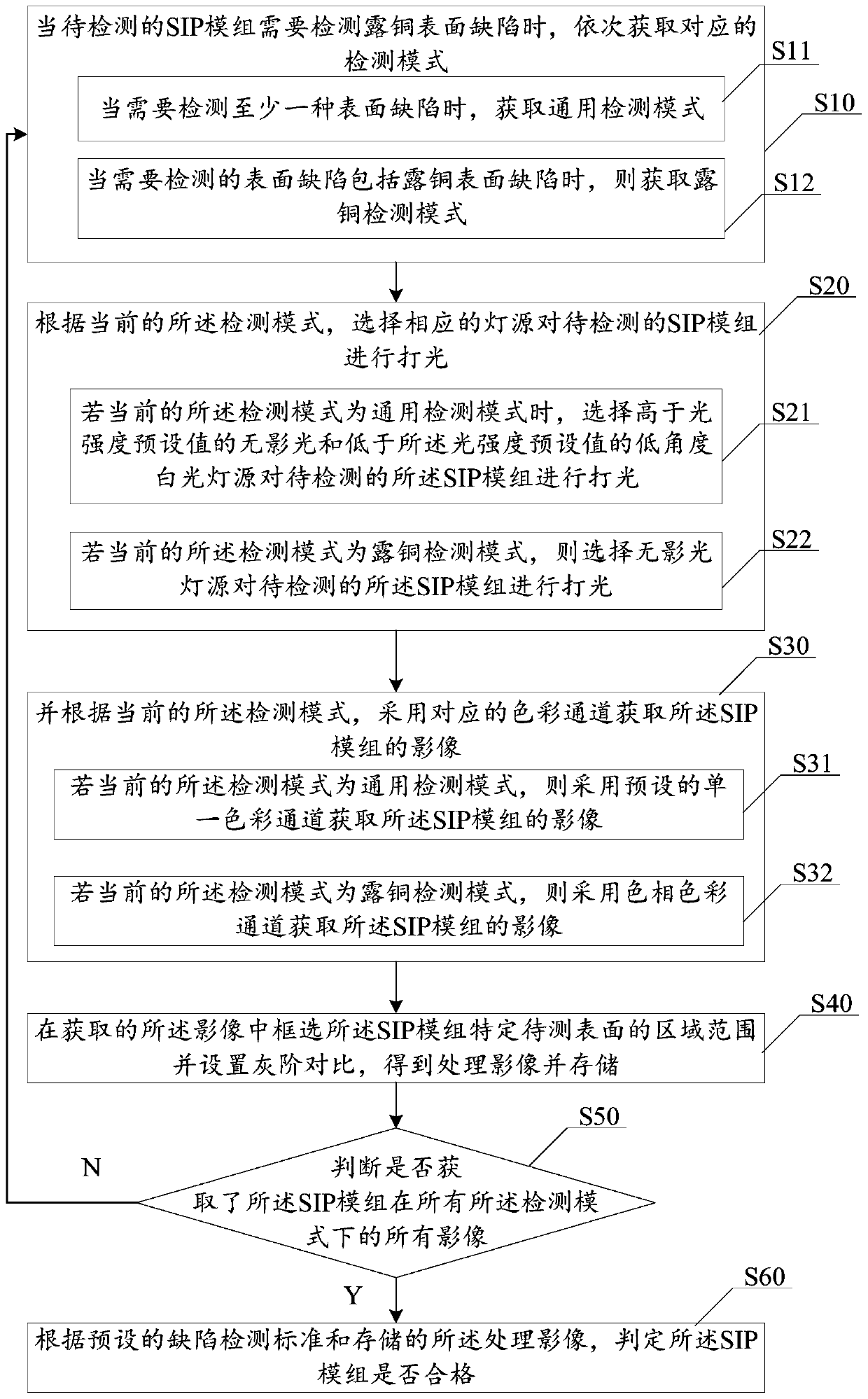
[0038] In order to more clearly illustrate the embodiments of the present invention or the technical solutions in the prior art, the specific implementation manners of the present invention will be described below with reference to the accompanying drawings. Obviously, the accompanying drawings in the following description are only some embodiments of the present invention, and those skilled in the art can obtain other accompanying drawings based on these drawings and obtain other implementations.

[0039] In order to make the drawing concise, each drawing only schematically shows the parts related to the present invention, and they do not represent the actual structure of the product. In addition, to make the drawings concise and easy to understand, in some drawings, only one of the components having the same structure or function is schematically shown, or only one of them is marked. Herein, "a" not only means "only one", but also means "more than one".

[0040] In one emb...


PUM


Abstract

The invention discloses a method and a system for detecting SIP module surface defects and exposed copper surface defects. The method comprises the following steps: S10, when exposed copper surface defects need to be detected, sequentially acquiring corresponding detection modes; S20, according to a current detection mode, selecting a corresponding light source to light an SIP module to be detected; S30, according to the current detection mode, acquiring an image of the SIP module by using a corresponding color channel; S40, circling an area range of a specific to-be-detected surface of the SIP module in the image acquired in the step S40, setting gray scale comparison so as to obtain a processed image, and storing the image; S50, judging whether all images of the SIP module in all detection modes are acquired or not, if yes, implementing a step S60, and if not, implementing a step S10; S60, judging whether the SIP module is qualified or not according to preset defect detection standards and stored processed images. By adoption of the method and the system, the product misjudgment rate can be reduced, and the volume production standard can be met.

Description

technical field [0001] The invention relates to the field of SIP module detection, in particular to a method and system for detecting SIP module surface defects and exposed copper surface defects. Background technique [0002] With the vigorous development of semiconductor technology, system-in-package (SIP, System In a Package) is the trend of packaging products now. SIP integrates multiple functional chips, including processors, memory and other functional chips, into one package to achieve A basically complete function. In the specific production process, the printed circuit board (PCB, Printed CircuitBoard) is made into PCBA (Printed Circuit Board Assembly) after surface mount technology (SMT, Surface Mount Technology), and then the upper surface of PCBA is filled with plastic encapsulation compound to form The molding layer (Molding) forms a SIP module after curing. PCB (Printed Circuit Board, printed circuit board) is a very important electronic component, a support ...

Claims


Application Information

Patent Timeline
Patent Type & Authority Patents(China)
IPC IPC(8): G01N21/95
Inventor 薛伯承林朝宣李冠儒李宗諭李冬冬
Owner UNIVERSAL SCIENTIFIC INDUSTRIAL (SHANGHAI) CO LTD
Why Eureka
Try Eureka