EDA (electronic design automation) and FPGA (field programmable gate array) reusable verification system for passive tag chips

A verification system and passive label technology, applied in the direction of instruments, electrical digital data processing, calculation, etc., can solve the problems of not meeting the standard requirements, hindering the development progress of labels, and lagging behind the development progress of labels, so as to avoid big risks Effect

Active Publication Date: 2016-11-09
WUXI KEYBRIDGE ELECTRONICS TECH CO LTD
View PDF5 Cites 4 Cited by
  • Summary
  • Abstract
  • Description
  • Claims
  • Application Information

AI Technical Summary

Problems solved by technology

[0002] The current mainstream EDA verification system in the industry such as figure 1 As shown, the module DUT to be verified is instantiated in the verification environment, and it is carried out by adding incentives to the DUT and observing the output of the DUT. Such a defect is that if the SV model of the reader written by the verification engineer is defective, it cannot be verified. There are also scenarios that verification engineers and design engineers ignore at the same time are difficult to find
[0003] Current mainstream FPGA verification systems in the industry such as figure 2 As shown, the practical physical product reader communicates with the tag RTL code downloaded to the FPGA board for verification through the antenna. The defect of this system is that all scenarios of the physical product reader are only a small part of the verification space, and all parameters have been verified. If it is fixed or changes too little or too much, it does not meet the standard requirements. In addition, the development progress of the reader may lag behind the development progress of the label. Such a verification system is too dependent on the reader manufacturer, which seriously hinders the development progress of the label.

Method used


Image

  • EDA (electronic design automation) and FPGA (field programmable gate array) reusable verification system for passive tag chips
  • EDA (electronic design automation) and FPGA (field programmable gate array) reusable verification system for passive tag chips
  • EDA (electronic design automation) and FPGA (field programmable gate array) reusable verification system for passive tag chips

Examples


Embodiment Construction

[0040] All features disclosed in this specification, or steps in all methods or processes disclosed, may be combined in any manner, except for mutually exclusive features and / or steps.

[0041] Any feature disclosed in this specification (including any appended claims, abstract and drawings), unless expressly stated otherwise, may be replaced by alternative features which are equivalent or serve a similar purpose. That is, unless expressly stated otherwise, each feature is one example only of a series of equivalent or similar features.

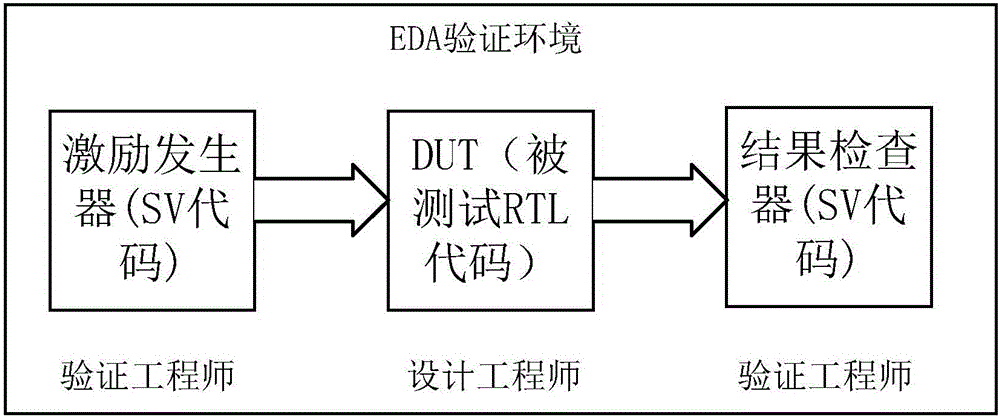
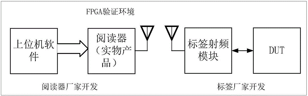
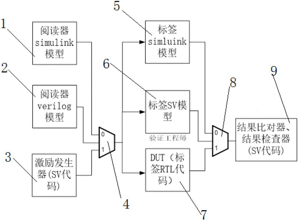
[0042] Such as image 3 with 5 As shown, an EDA and FPGA reusable verification system for passive tag chips: including EDA environment verification system and FPGA environment verification system;

[0043] Reader simulink model 1 in the described EDA environment verification system, reader verilog model 2 and excitation generator 3 are connected with the input end of selection controller-4, and the output end of selection controller 4 is con...


PUM


Abstract

The invention relates to an EDA (electronic design automation) and FPGA (field programmable gate array) reusable verification system for passive tag chips. The EDA and FPGA reusable verification system comprises an EDA environment verification system and an FPGA environment verification system. A reader verilog model (2) and a DUT (device under test) (7) in the EDA environment verification system and a reader verilog model (1-3) and a DUT (1-10) in the FPGA environment verification system can be reused mutually. The EDA and FPGA reusable verification system has the advantages that the readers and verilog codes of tags can be reused in EDA and FPGA verification environments in the verification systems, accordingly, codes for EDA and FPGA are identical, RTL (resistor transistor logic) codes do not need to be modified between the two verification systems, and high risks due to little modification can be prevented.

Description

technical field [0001] The invention relates to an EDA and FPGA reusable verification system for passive tag chips. Background technique [0002] The current mainstream EDA verification system in the industry such as figure 1 As shown, the module DUT to be verified is instantiated in the verification environment, and it is carried out by adding incentives to the DUT and observing the output of the DUT. Such a defect is that if the SV model of the reader written by the verification engineer is defective, it cannot be verified. There are also scenarios that are overlooked by both the verification engineer and the design engineer and are hard to spot. [0003] Current mainstream FPGA verification systems in the industry such as figure 2 As shown, the practical physical product reader communicates with the tag RTL code downloaded to the FPGA board for verification through the antenna. The defect of this system is that all scenarios of the physical product reader are only a sm...

Claims


Application Information

Patent Timeline
IPC IPC(8): G06F11/36
CPCG06F11/3652G06F11/3656
Inventor 蔡友向晓安张建王立泉
Owner WUXI KEYBRIDGE ELECTRONICS TECH CO LTD
Why Eureka
Try Eureka