Terminal structure of superconducting cable and manufacturing method thereof
A technology for superconducting cables and structures, which is applied in the manufacture of cables/conductors, the usage of superconductor elements, and superconducting devices, etc., can solve the problems of deviation of connection resistance, cumbersome, cumbersome production of normally conducting connecting parts, etc. The effect of contact resistance
- Summary
- Abstract
- Description
- Claims
- Application Information
AI Technical Summary
Problems solved by technology
Method used
Image
Examples
Embodiment 1
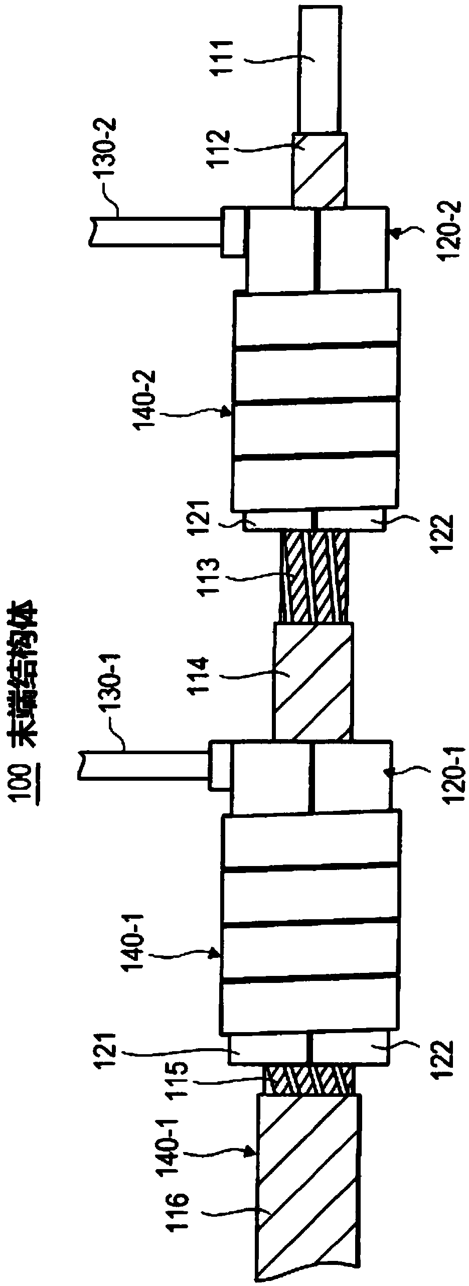
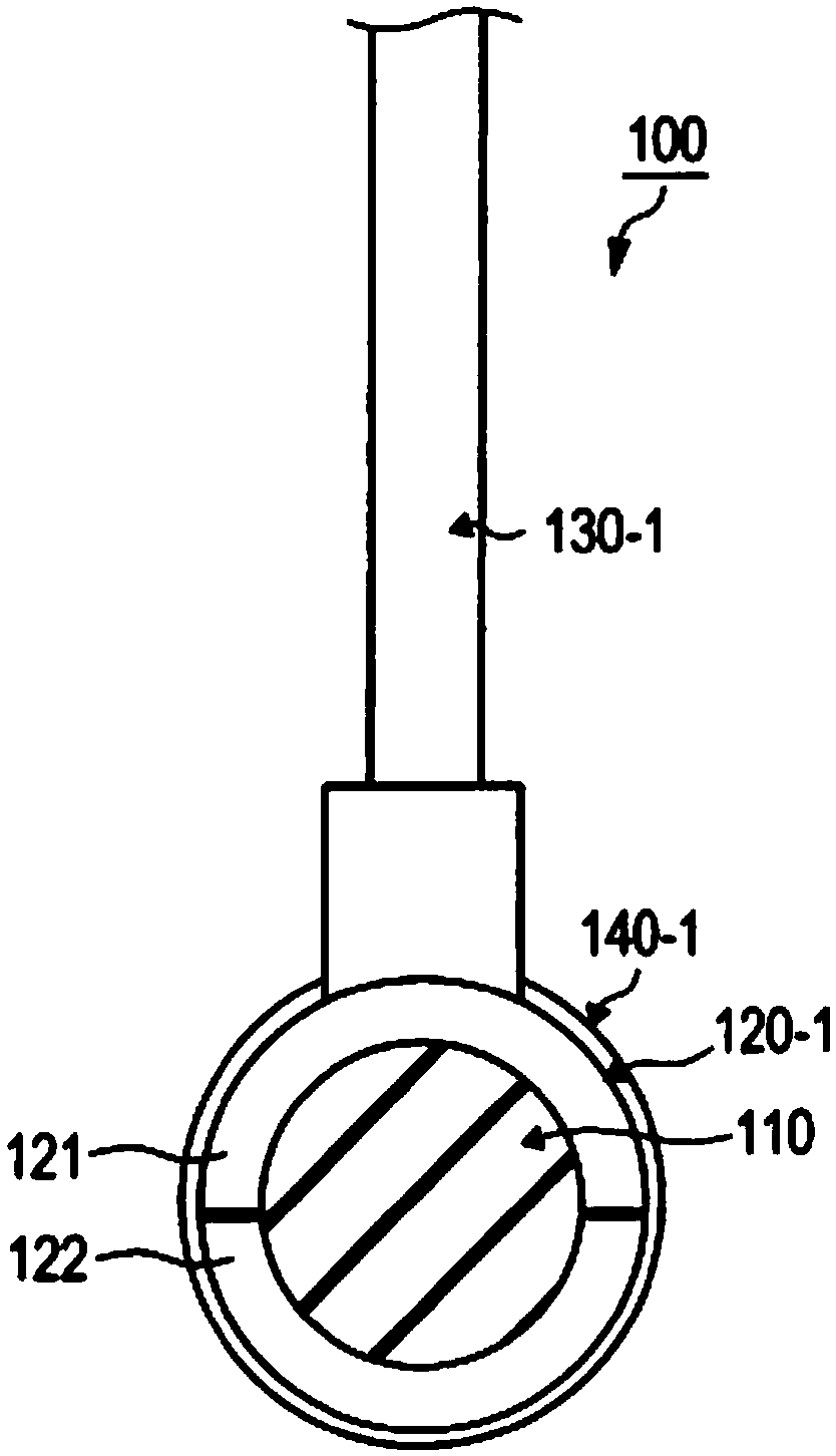
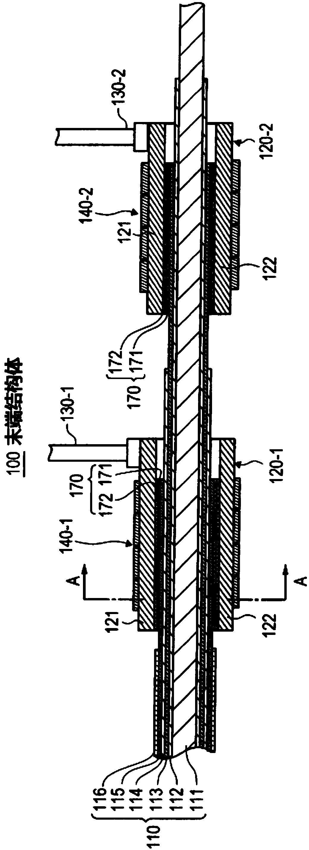
[0117] Formed with thickness 0.12[mm]×width 5[mm] Figure 5 REBa shown y Cu 3 o z It is a superconducting wire, and 10 of the superconducting wires are wound around the core material to form each layer of the superconducting tape to form a superconducting cable. Using the superconducting cable, cylindrical electrodes, and diameter-reducing parts, the above-mentioned structure was manufactured. End structure 100 . The inner surface of the cylindrical electrode 120 - 1 and the outer peripheral surface (surface on the substrate side) of the superconducting tape 115 are connected by solder 170 . In addition, when the tubular electrode 120 is connected to the superconducting strip 115, pre-solder portions 171 and 172 are provided on the connection surfaces of the two, such as Figure 9 to Figure 14 They were fabricated as shown.
PUM
| Property | Measurement | Unit |
|---|---|---|
| thickness | aaaaa | aaaaa |
| width | aaaaa | aaaaa |
Abstract
Description
Claims
Application Information
 - R&D Engineer
- R&D Manager
- IP Professional
- Industry Leading Data Capabilities
- Powerful AI technology
- Patent DNA Extraction
Browse by: Latest US Patents, China's latest patents, Technical Efficacy Thesaurus, Application Domain, Technology Topic, Popular Technical Reports.
© 2024 PatSnap. All rights reserved.Legal|Privacy policy|Modern Slavery Act Transparency Statement|Sitemap|About US| Contact US: help@patsnap.com


