
Pixel structure, liquid crystal display panel and drive method of liquid crystal display panel

A liquid crystal display panel, pixel structure technology, applied in nonlinear optics, instruments, optics, etc., can solve the problems of difficult to achieve narrow borders, occupied area, etc., and achieve the effect of increasing the aperture ratio

Inactive Publication Date: 2016-10-12
TCL CHINA STAR OPTOELECTRONICS TECH CO LTD
View PDF9 Cites 3 Cited by
  • Summary
  • Abstract
  • Description
  • Claims
  • Application Information

AI Technical Summary

Problems solved by technology

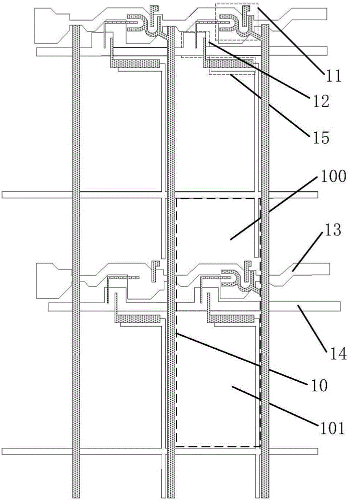
Since the shared gate 14 of the nth row is connected to the charging gate 13 of the n+4 row at the periphery, it occupies the peripheral design area and it is difficult to achieve a narrow border

Method used


Image

  • Pixel structure, liquid crystal display panel and drive method of liquid crystal display panel
  • Pixel structure, liquid crystal display panel and drive method of liquid crystal display panel
  • Pixel structure, liquid crystal display panel and drive method of liquid crystal display panel

Examples


Embodiment Construction

[0022] The following will clearly and completely describe the technical solutions in the embodiments of the present invention in conjunction with the accompanying drawings in the embodiments of the present invention. Obviously, the described embodiments are only some of the embodiments of the present invention, not all of them. Based on the embodiments of the present invention, all other embodiments obtained by persons of ordinary skill in the art without making creative efforts belong to the protection scope of the present invention.

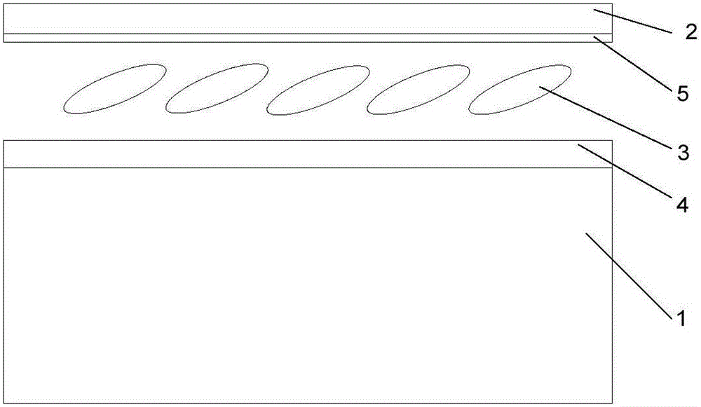
[0023] figure 2 is a schematic structural diagram of a liquid crystal display panel according to an embodiment of the present invention. like figure 2 As shown, the liquid crystal display panel includes an array substrate 1, a color filter substrate 2 disposed opposite to the array substrate 1, and a liquid crystal layer 3 sandwiched between the array substrate 1 and the color filter substrate 2, and the pixel electrodes 4 are arranged on th...


PUM


Abstract

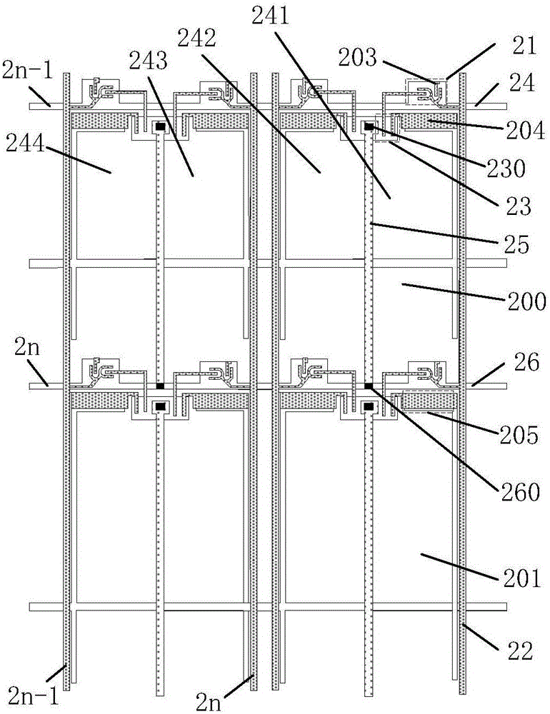
The invention discloses a pixel structure, a liquid crystal display panel and a drive method of the liquid crystal display panel. The pixel structure comprises a plurality of pixels arrayed in a matrix mode. Each pixel comprises a main pixel region and an auxiliary pixel region which are adjacently arranged, wherein the main pixel region comprises a first pixel electrode connected with a data line through a first control switch, and the auxiliary pixel region comprises a second pixel electrode connected with a data line through a second control switch and the first control switch. The first control switch is controlled through a first scanning line, the second control switch is controlled through a charge sharing line, and the charge sharing line is connected with the second scanning line different from the first scanning line. In this way, the aperture opening ratios of the pixels can be increased, peripheral design regions are not occupied, and narrow-side frames can be achieved easily.

Description

technical field [0001] The invention relates to the technical field of liquid crystal display, in particular to a pixel structure, a liquid crystal display panel and a driving method thereof. Background technique [0002] Thin Film Transistor (TFT)-Liquid Crystal Display (LCD) relies on liquid crystals to have different orientations in different electric fields. At this time, due to the optical birefringence of liquid crystals, the backlight will be introduced into the liquid crystal. Different light produces different transmittances, and then produces gray scales. By placing red, green and blue (RGB) color-resistors on the optical path, you can get different colors and different bright and dark pictures. When viewing a liquid crystal display at a large viewing angle, due to different angles, the transmittance in each direction is also different, and the perceived deviation value is also different, so the phenomenon called color shift (color shift) in the industry occurs. I...

Claims


Application Information

Patent Timeline
Patent Type & Authority Applications(China)
IPC IPC(8): G02F1/1362G02F1/1368
CPCG02F1/13624G02F1/136286G02F1/1368G02F1/134309G02F1/134336G02F1/134345G02F2201/123G02F1/136295
Inventor 孙博邹晓灵
Owner TCL CHINA STAR OPTOELECTRONICS TECH CO LTD
Learn More