FPGA implementation method of SMV/GOose message based on rmii interface
An implementation method and interface technology, applied in the direction of synchronous signal speed/phase control, digital transmission system, data exchange network, etc., can solve the problems of increasing the cost of the merged unit, difficulty in hardware layout and wiring, and obstacles to the upgrade of the merged unit.
- Summary
- Abstract
- Description
- Claims
- Application Information
AI Technical Summary
Problems solved by technology
Method used
Image
Examples
Embodiment Construction
[0031] The present invention will be further described below in conjunction with the accompanying drawings and embodiments.
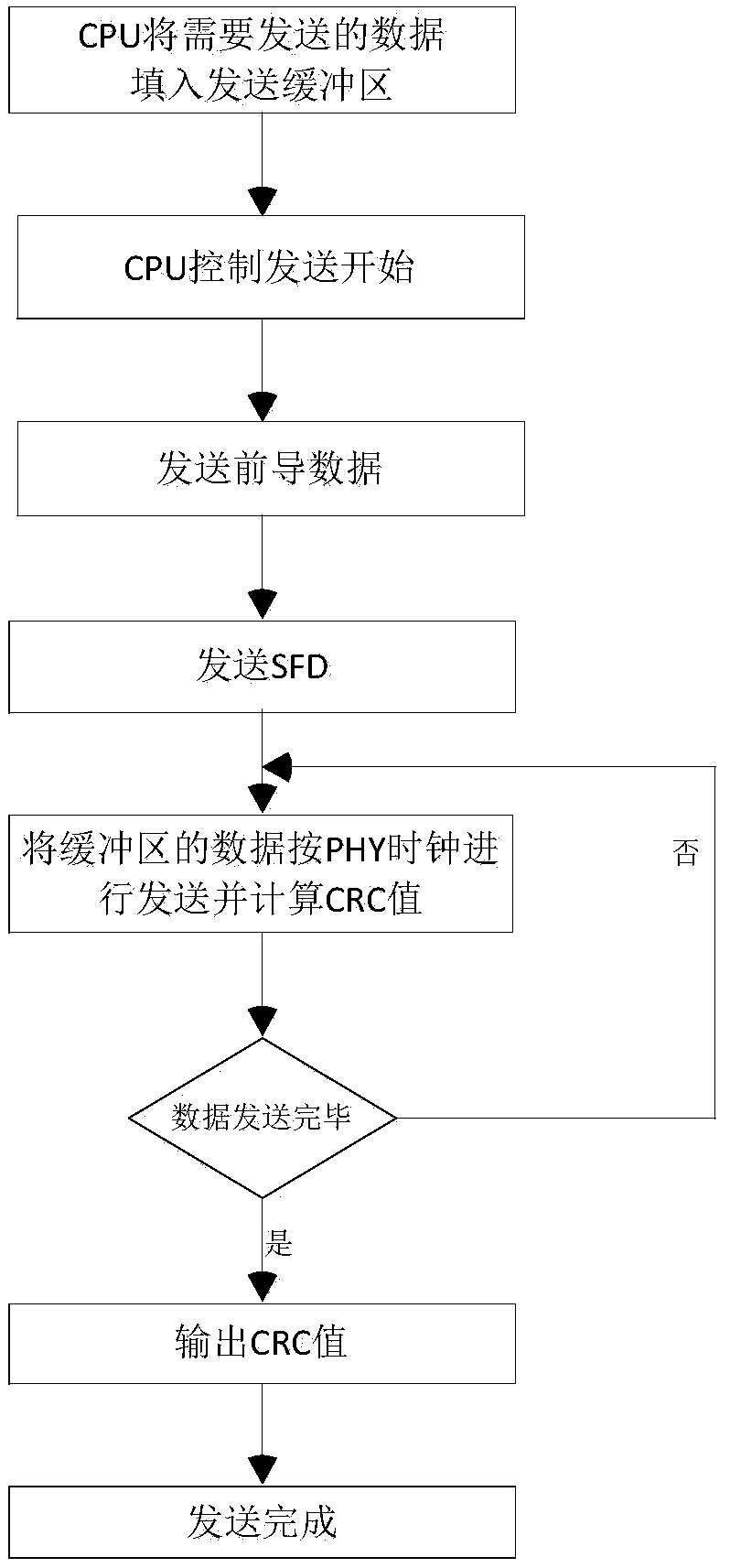
[0032] Such as figure 1 As shown, the FPGA implementation method of the SMV / GOOSE message based on the RMII interface includes:
[0033] Step 1: Initialize the FPGA internal registers, buffer the message data to the sending buffer; wait for the sending enable signal;
[0034] Step 2: After receiving the enable signal, the transmit enable terminal TX_EN is pulled high to enter the data transmission state; whenever the PHY chip clock falls, 2-bit data is sent through the TXD[1:0] (transmit data line) port, and every time the When one byte is finished, the counter is incremented by one; firstly send 7 bytes of "0x55" (Preamble) for the receiver to realize synchronization and extract clock information, and then send 1 byte of "0xd5" (SFD) to use At the start of notifying the receiver of valid data;
[0035] Step 3: Send the message data in the buffer to ...
PUM
 Abstract
Description
Claims
Application Information
 - Generate Ideas
- Intellectual Property
- Life Sciences
- Materials
- Tech Scout
- Unparalleled Data Quality
- Higher Quality Content
- 60% Fewer Hallucinations
Browse by: Latest US Patents, China's latest patents, Technical Efficacy Thesaurus, Application Domain, Technology Topic, Popular Technical Reports.
© 2025 PatSnap. All rights reserved.Legal|Privacy policy|Modern Slavery Act Transparency Statement|Sitemap|About US| Contact US: help@patsnap.com


