
A contact image sensor and image scanning device

An image scanning device and image sensor technology, applied in image communication, instruments, optics, etc., can solve the problems of increasing the size of the scanning device, increasing the cost, etc., and achieve high-resolution scanning, high-resolution scanning, and resolution improvement. Effect

Active Publication Date: 2019-02-19
WEIHAI HUALING OPTO ELECTRONICS CO LTD
View PDF7 Cites 0 Cited by
  • Summary
  • Abstract
  • Description
  • Claims
  • Application Information

AI Technical Summary

Problems solved by technology

This not only increases the volume of the scanning device, but also greatly increases the cost

Method used


Image

  • A contact image sensor and image scanning device
  • A contact image sensor and image scanning device
  • A contact image sensor and image scanning device

Examples


Embodiment 1

[0028] Figure 5 A schematic structural diagram of the image scanning device shown in Embodiment 1 is shown. The main difference between the image scanning device and the existing image scanning device is that the image scanning device includes two new contact image sensors involved in the present invention, that is, the first contact image sensor X1 and the second contact image sensor Y1 . The first contact image sensor X1 is placed parallel to the X direction of the image scanning device, the second contact image sensor Y1 is placed parallel to the Y direction of the image scanning device, and the first contact image sensor X1 is pulled by the first traction mechanism 21, The second contact image sensor Y1 is pulled by the second pulling mechanism 22 , and the image scanning device further includes a control system 23 , a post-processing system 24 and a document table 25 . The control system 23 is mainly used to control the normal operation of the first contact image sensor...

Embodiment 2

[0031] Figure 6 A schematic structural diagram of the image scanning device shown in Embodiment 2 is shown. The difference between this embodiment and Embodiment 1 is that the image scanning device adopts a new contact image sensor involved in the present invention, such as the first contact image sensor X1, and a rotating device 26 is added. Its working principle is as follows: under the control of the control system 23 , the first traction mechanism 21 pulls the first contact image sensor X1 along the Y direction with a step of a / N, so as to obtain a set of data in the Y direction. After the first contact image sensor X1 completes scanning along the Y direction, under the action of the rotating device 26, the first contact image sensor X1 rotates 90 degrees, parallel to the Y direction, the first traction mechanism 21 is controlled by the control system 23 Pull down the first contact image sensor X1 and scan along the X direction to obtain a set of data in the X direction....


PUM


Abstract

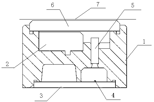
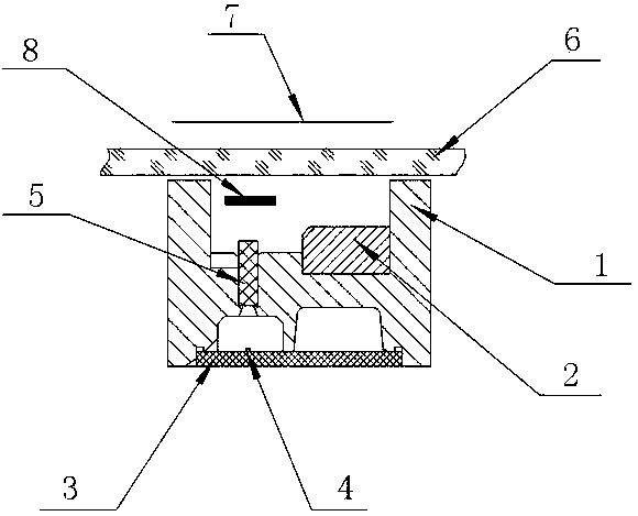
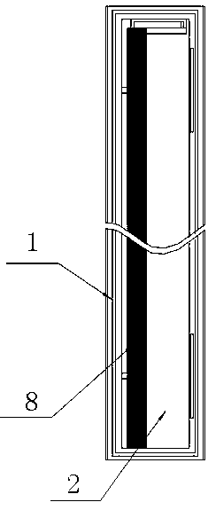
The present invention proposes a contact image sensor, which includes a light source, a lens, a photosensitive part that receives the light collected by the lens, a sensor substrate equipped with photosensitive integrated circuits arranged in a line, a frame for accommodating the lens and the sensor substrate, and is arranged on the upper part of the frame. The contact image sensor also includes a linear magnifying glass on the light-transmitting plate carrying the original, the linear magnifying glass is arranged between the light-transmitting plate and the lens, and the linear magnifying glass can linearly enlarge the object in a single direction. characteristics. The contact image sensor according to the present invention can improve the resolution in one direction.

Description

technical field [0001] The invention relates to the field of contact image sensors, in particular to a contact image sensor and an image scanning device which use a linear magnifying glass to improve scanning resolution. Background technique [0002] With the popularization of computerized office, the application of scanning devices is becoming more and more extensive. We can use scanning devices to scan pictures, documents, etc., and then input them into computers for later editing or storage. Scanning resolution is an important indicator of scanning devices. If the resolution is too low, the scanned image may not meet the needs of subsequent processing. [0003] However, the scanning accuracy of existing scanning devices mainly depends on the accuracy of optical components. For example, the resolution of a contact image sensor (CIS) is determined by the resolution of its photosensitive chip (IC). Taking a 600DPI IC as an example, The size of its photosensitive window is ...

Claims


Application Information

Patent Timeline
Patent Type & Authority Patents(China)
IPC IPC(8): H04N1/031H04N1/04
CPCH04N1/031H04N1/0314H04N1/0443H04N1/0452H04N1/04H04N1/387G02B26/101G02B3/08H04N1/3877H04N1/3935
Inventor 张文波王虎岩
Owner WEIHAI HUALING OPTO ELECTRONICS CO LTD
Learn More