Probe antenna for terahertz waveband near-field imaging
A near-field imaging, terahertz technology, applied in the direction of the antenna grounding switch structure connection, the structure of the radiating element, etc., can solve the problems of low efficiency of the probe antenna and difficult mechanical manufacturing, and achieve the enhancement of the input electric field and the simple mechanical manufacturing. Effect
- Summary
- Abstract
- Description
- Claims
- Application Information
AI Technical Summary
Benefits of technology
Problems solved by technology
Method used
Image
Examples
Embodiment 1
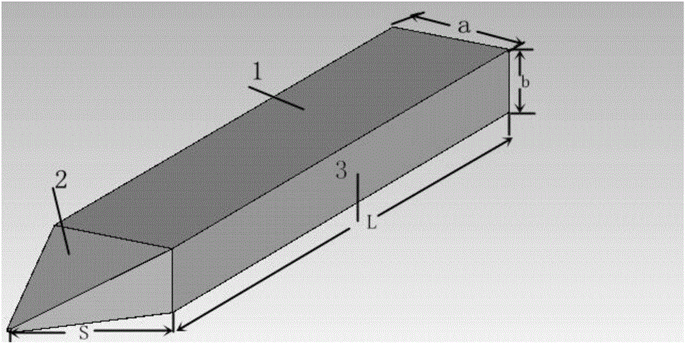
[0028] Embodiment 1: This example uses the three-dimensional electromagnetic field simulation software CST MICROWAVE STUDIO (Microwave Studio) of Germany CST (Computer Simulation Technology) company to carry out simulation analysis on this embodiment. First build a probe antenna model in the terahertz band in CST.
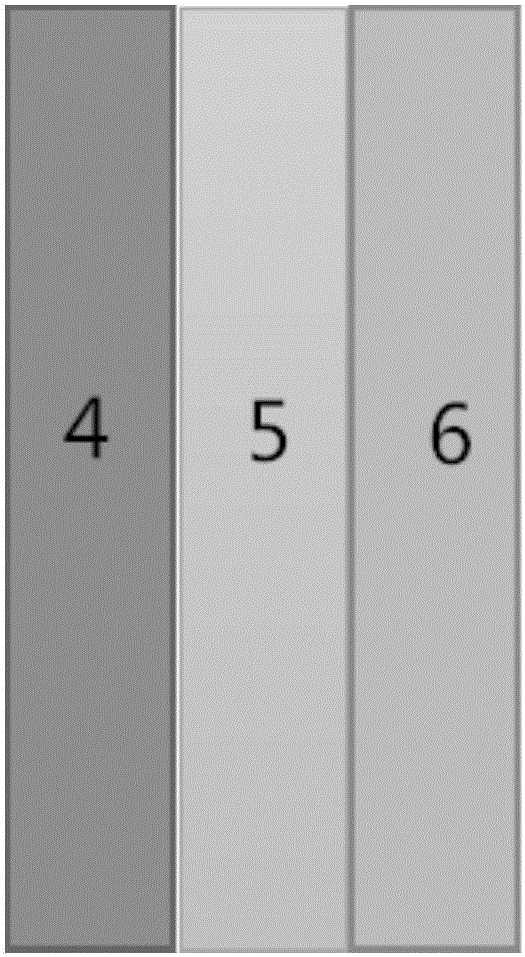
[0029] In this example, the antenna is prepared in the following way: first step, the terahertz coupling input part and the terahertz resonant cavity cavity of the required size are made by micro-nano processing technology; The narrow sides of the waveguide and the terahertz resonant cavity are coated with metal on the surface. From the inside to the outside, there are titanium bonding layer, aluminum working layer and gold protection layer respectively, and then the required terahertz wave near-field probe antenna is made.
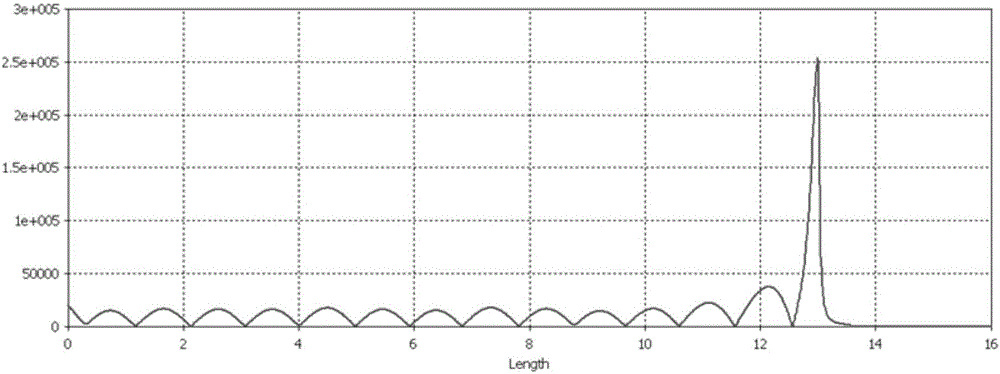
[0030] like figure 1 and 2 As shown, this example includes a terahertz coupling input part 1 , a terahertz resonant cavity 2 , a PMMA surfa...
Embodiment 2
[0041] Embodiment 2: In this embodiment, the beam size of the transmitting end of the antenna is related to the ratio of the cross-section of the needle tip port. When other external conditions remain unchanged, such as Figure 8 As shown, only change the length-to-width ratio of the tip end cross-section to 0.02x1mm 2 , the Y-O-Z interface whose electric field strength propagates inside the antenna is as Figure 9 As shown, the beam width at the tip tip is proportional to the port width.
PUM
| Property | Measurement | Unit |
|---|---|---|
| Length | aaaaa | aaaaa |
| Length | aaaaa | aaaaa |
Abstract
Description
Claims
Application Information
 - R&D
- Intellectual Property
- Life Sciences
- Materials
- Tech Scout
- Unparalleled Data Quality
- Higher Quality Content
- 60% Fewer Hallucinations
Browse by: Latest US Patents, China's latest patents, Technical Efficacy Thesaurus, Application Domain, Technology Topic, Popular Technical Reports.
© 2025 PatSnap. All rights reserved.Legal|Privacy policy|Modern Slavery Act Transparency Statement|Sitemap|About US| Contact US: help@patsnap.com


