Array substrate, manufacturing method thereof, and display device
A technology for array substrates and manufacturing methods, which is applied in the display field and can solve problems such as low light transmittance of array substrates
- Summary
- Abstract
- Description
- Claims
- Application Information
AI Technical Summary
Problems solved by technology
Method used
Image
Examples
Embodiment 1
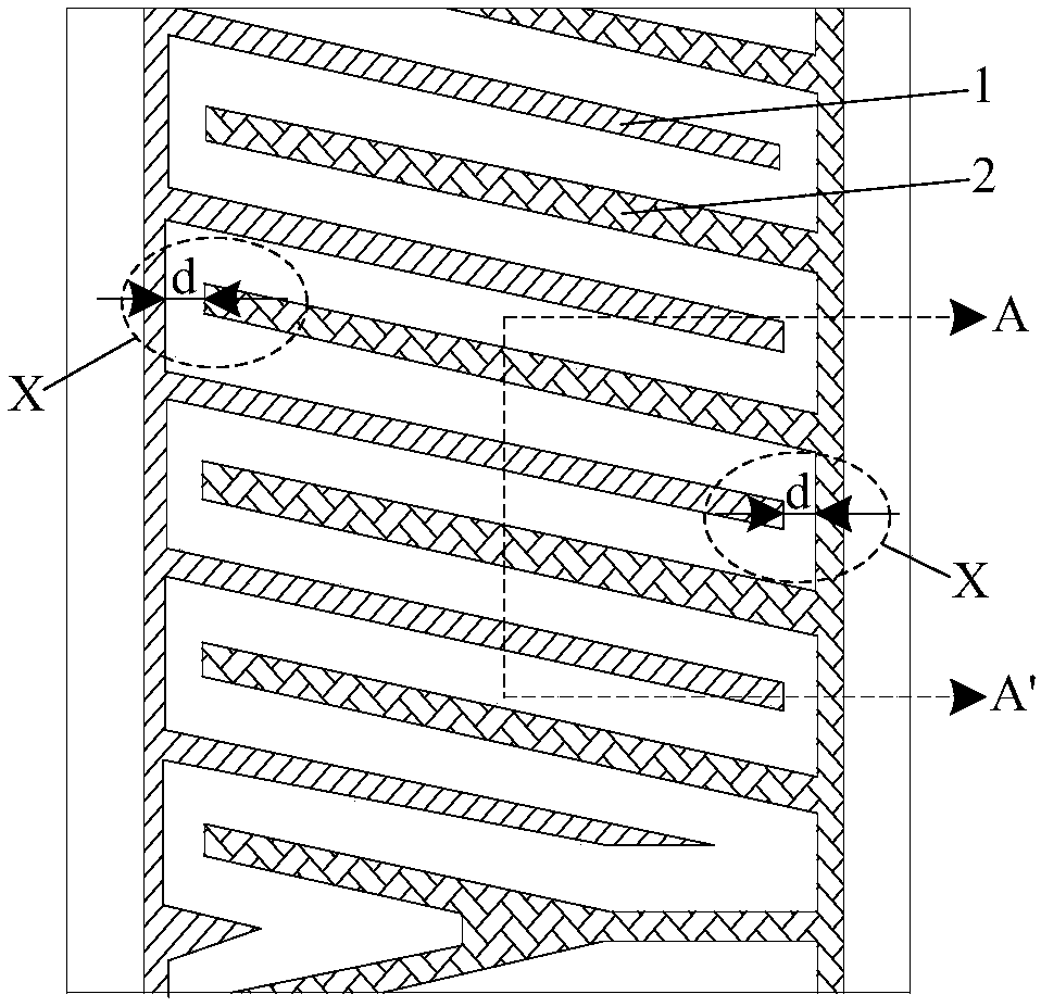
[0027] As mentioned in the background art, the array substrate using the comb electrode structure in the prior art has the problem of low light transmittance. The inventors of the present invention have found through research that one of the reasons for the above-mentioned problem is: as figure 1 and 2 As shown, since the pixel electrode 1 and the common electrode 2 are formed in the same patterning process in the prior art, the electrode material between the pixel electrode 1 and the common electrode 2 is etched to form the pattern of the pixel electrode 1 and the common electrode 2 In the process, limited by the process capability, there will be electrode material residue between the pixel electrode 1 and the common electrode 2. end, ie figure 1 The X shown in is especially serious. If the gap d between the pixel electrode 1 and the common electrode 2 at X is too small, there will be more electrode material remaining between the two at X, causing the two to be unable to b...
Embodiment 2
[0048] This embodiment provides an array substrate, such as Figure 6 As shown, the array substrate includes: a base substrate 3, a first electrode 6 disposed on the base substrate 3, a passivation layer 5 covering the first electrode 6 and roughly the same shape as the first electrode 6, disposed on the substrate The second electrode 8 on the base substrate 3 . Wherein, an electric field can be formed between the first electrode 6 and the second electrode 8 , and the electric field may include a horizontal electric field parallel to the base substrate 3 for driving liquid crystal molecules to deflect.
[0049] In the above array substrate, since the passivation layer 5 and the first electrode 6 have approximately the same shape, the passivation layer 5 and the first electrode 6 can be formed in the same patterning process, and since the passivation layer 5 covers the first Therefore, the first electrode 6 and the second electrode 8 can be formed in different patterning proce...
Embodiment 3
[0059] This embodiment provides a display device, which includes the array substrate as described in the second embodiment. Since the gap between the first electrode and the second electrode in the array substrate described in the second embodiment can be set smaller, the light transmittance is higher, and the signal crosstalk between the first electrode and the second electrode is acceptable. Therefore, the display device including the array substrate also has the advantages of high light transmittance and signal crosstalk within an acceptable range.
[0060] It should be noted that the display device provided in this embodiment is preferably a liquid crystal display device, specifically any product with a display function such as a liquid crystal panel, a mobile phone, a tablet computer, a television, a monitor, a notebook computer, a digital photo frame, a navigator, etc. or parts.
PUM
 Abstract
Description
Claims
Application Information
 - R&D
- Intellectual Property
- Life Sciences
- Materials
- Tech Scout
- Unparalleled Data Quality
- Higher Quality Content
- 60% Fewer Hallucinations
Browse by: Latest US Patents, China's latest patents, Technical Efficacy Thesaurus, Application Domain, Technology Topic, Popular Technical Reports.
© 2025 PatSnap. All rights reserved.Legal|Privacy policy|Modern Slavery Act Transparency Statement|Sitemap|About US| Contact US: help@patsnap.com


