Manufacturing method of flexible substrate

A technology of flexible substrates and manufacturing methods, which is applied in the direction of electrical components, electrical solid devices, circuits, etc., can solve the problems of flexible device corrosion, flexible substrate damage, excessive temperature, etc., and achieve reduced production costs, efficient stripping, and improved yields Effect

Inactive Publication Date: 2016-07-27
WUHAN CHINA STAR OPTOELECTRONICS TECH CO LTD
View PDF6 Cites 1 Cited by
  • Summary
  • Abstract
  • Description
  • Claims
  • Application Information

AI Technical Summary

Problems solved by technology

[0004] At this stage, many companies and scientific research institutions in the display industry have proposed different solutions for this technology. For example, LG uses a chemical method to etch the stainless steel substrate to achieve the peeling off of the flexible substrate and the rigid substrate. It also has a corrosive effect, which greatly reduces the lifespan of flexible displays
Samsung adopts resistance heating sense detachment technology, which uses heating to detach the substrate from the glass, but the high temperature and the need to protect the light-emitting device, resulting in the yield and cost cannot be guaranteed
However, although the separation of the flexible substrate and the rigid substrate has been achieved, the separation of the flexible substrate and the second rigid substrate will face the same peeling problem, and it is easy to cause damage to the flexible substrate.

Method used


Image

  • Manufacturing method of flexible substrate
  • Manufacturing method of flexible substrate
  • Manufacturing method of flexible substrate

Examples


Embodiment Construction

[0032] In order to further illustrate the technical means adopted by the present invention and its effects, the following describes in detail in conjunction with preferred embodiments of the present invention and accompanying drawings.

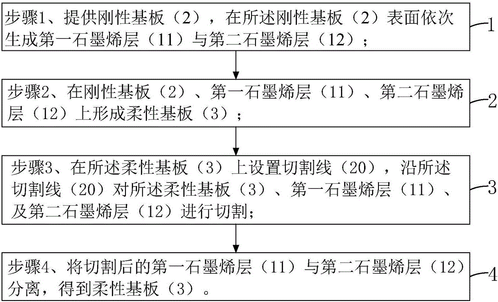
[0033] see figure 1 , the present invention provides a method for manufacturing a flexible substrate, comprising the following steps:

[0034] Step 1, such as Figure 2-4 As shown, a rigid substrate 2 is provided, and a first graphene layer 11 and a second graphene layer 12 are sequentially formed on the surface of the rigid substrate 2 .

[0035] The specific implementation of described step 1 comprises the following steps:

[0036] Step 11, such as figure 2 As shown, a substrate 1 is provided, and a first graphene layer 11 is formed on the surface of the substrate 1 .

[0037] Specifically, the material of the substrate 1 is metal; the step 11 adopts a chemical vapor deposition (Chemical Vapor Deposition, CVD) method under high temperat...


PUM


Abstract

The invention provides a manufacturing method of a flexible substrate. The method comprises the steps of: 1, providing a rigid substrate, successively generating a first grapheme layer and a second grapheme layer on the surface of the rigid substrate; 2, forming a flexible substrate on the rigid substrate, the first grapheme layer and the second grapheme layer; 3, carrying out cutting along the edges of the flexible substrate; and 4, separating the first t grapheme layer from the second grapheme layer, and obtaining the flexible substrate retaining the second grapheme layer on the bottom surface. Compared with the prior art, the lossless, mild and high-efficiency peeling between the flexible substrate and the rigid substrate is realized, the second grapheme layer retained on the bottom surface of the flexible substrate has no influences on the flexible substrate, the production cost is effectively lowered, and the yield rate of the production process is improved.

Description

technical field [0001] The invention relates to the field of display technology, in particular to a method for manufacturing a flexible substrate. Background technique [0002] With the continuous updating and development of science and technology, bendable flexible devices made of flexible substrates are expected to become the mainstream equipment of the next generation of optoelectronic devices, such as displays, chips, circuits, power supplies, sensors and other flexible devices can achieve what traditional optoelectronic devices cannot The functions realized have great advantages in terms of cost and user experience. Taking flexible display as an example, it is a method of preparing devices on the surface of a substrate made of flexible materials, such as flexible active-matrix organic light emitting diodes (Active-matrix organic light emitting diode, AMOLED), which need to be prepared or adsorbed on the surface of a rigid substrate. substrate, followed by device fabric...

Claims


Application Information

Patent Timeline
Patent Type & Authority Applications(China)
IPC IPC(8): H01L27/12H01L27/32
CPCH01L27/1266H10K59/12H10K71/80H10K59/1201
Inventor 王选芸
Owner WUHAN CHINA STAR OPTOELECTRONICS TECH CO LTD
Why Eureka
Try Eureka