A hybrid multi-core planar optical waveguide structure and its coupling structure and coupling method
A planar optical waveguide and main waveguide technology, applied in the field of optical waveguide coupling, can solve the problems of high packaging cost, complex process, large-scale integration difficulties, etc., and achieve the effect of improving coupling efficiency and alignment tolerance.
- Summary
- Abstract
- Description
- Claims
- Application Information
AI Technical Summary
Problems solved by technology
Method used
Image
Examples
Embodiment 1
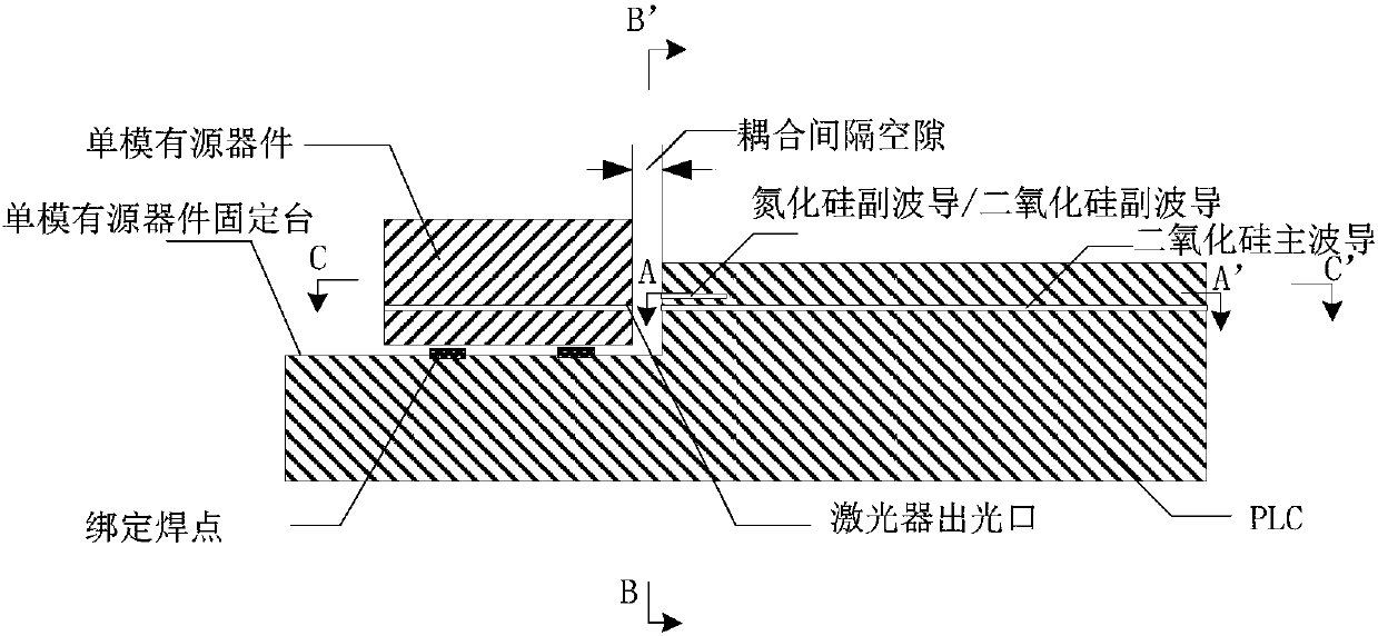
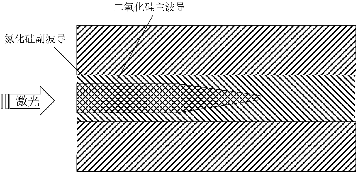
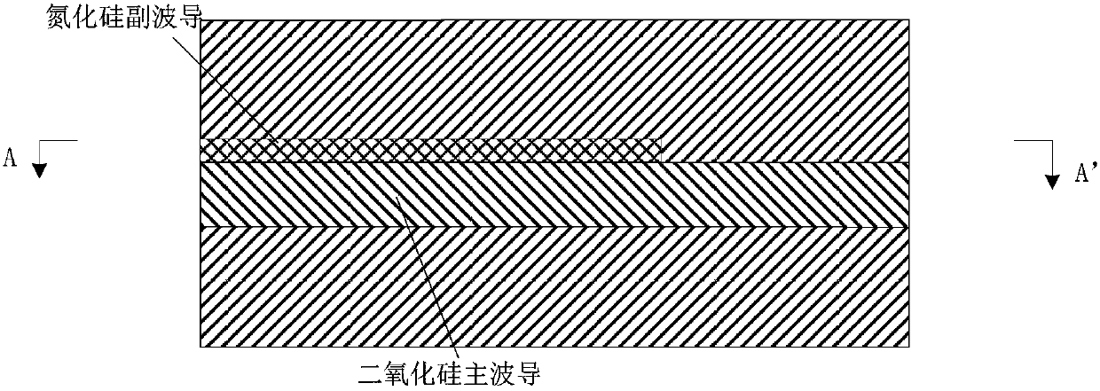
[0057] Embodiment 1 of the present invention provides a hybrid multi-core planar optical waveguide structure, such as Figure 1-4 The structure includes, specifically:
[0058] The planar optical waveguide includes a silicon dioxide main waveguide for transmitting optical signals, and a secondary waveguide for assisting light entering;
[0059] The secondary waveguide includes a silicon nitride secondary waveguide, and the silicon nitride secondary waveguide is in close contact with the silicon dioxide main waveguide.
[0060] Wherein, the silicon nitride secondary waveguide can be in various structural forms: for example, it is specifically a rectangular cubic structure, a positive ladder structure, an inverted ladder structure, and the like.
[0061] The hybrid multi-core waveguide proposed in this embodiment refers to adding a silicon nitride secondary waveguide other than the silicon dioxide main waveguide to the laser interface of the PLC to form a hybrid multi-core wave...
Embodiment 2
[0065] Based on the planar optical waveguide structure described in Embodiment 1, Embodiment 2 of the present invention specifically elaborates one of the optional sub-waveguide structures. Specifically, the sub-waveguide not only includes a silicon nitride sub-waveguide, but also includes Silica secondary waveguides, such as Figure 5 , Figure 6 , Figure 7 and Figure 8 As shown, the specific structure is described as follows:
[0066] The planar optical waveguide includes a silicon dioxide main waveguide for transmitting optical signals, and a secondary waveguide for assisting light entering;
[0067] Both the silicon nitride secondary waveguide and the silicon dioxide secondary waveguide are composed of a transition part and a cone part. The transition part is a rectangular cube extending toward the light transmission direction; A structure extending in the light transmission direction; wherein, the silicon nitride secondary waveguide is located on the upper surface o...
Embodiment 3
[0085] Based on the planar optical waveguide structure described in Embodiment 1, Embodiment 3 of the present invention specifically elaborates one of the optional secondary waveguide structures, such as Figure 10 , Figure 11 and Figure 12 As shown, specifically, the silicon nitride sub-waveguide is composed of two sub-sub-waveguides, wherein the first sub-sub-waveguide is located on the upper surface of the silicon dioxide main waveguide, and the second sub-sub-waveguide is located on the silicon dioxide The lower surface of the main waveguide.
[0086] In combination with the embodiment of the present invention, there is a preferred implementation solution, such as Figure 10 As shown, both the first sub-waveguide and the second sub-waveguide are composed of a transition part and a cone part, wherein the transition part is a rectangular cube extending toward the light transmission direction; wherein the cone part is the bottom surface and the transition part Convergenc...
PUM
 Abstract
Description
Claims
Application Information
 - R&D
- Intellectual Property
- Life Sciences
- Materials
- Tech Scout
- Unparalleled Data Quality
- Higher Quality Content
- 60% Fewer Hallucinations
Browse by: Latest US Patents, China's latest patents, Technical Efficacy Thesaurus, Application Domain, Technology Topic, Popular Technical Reports.
© 2025 PatSnap. All rights reserved.Legal|Privacy policy|Modern Slavery Act Transparency Statement|Sitemap|About US| Contact US: help@patsnap.com


