
Semiconductor element positioning and turning device

A positioning steering and semiconductor technology, applied in the direction of conveyor objects, transportation and packaging, etc., can solve problems such as low work efficiency and complex structure, and achieve the effects of improving production efficiency, simplifying structure, and reducing costs

Inactive Publication Date: 2016-06-01
扬州泽旭电子科技有限责任公司
View PDF0 Cites 8 Cited by
  • Summary
  • Abstract
  • Description
  • Claims
  • Application Information

AI Technical Summary

Problems solved by technology

[0002] In the production process of semiconductor components, the direction of semiconductor components needs to be corrected before many processes. The correction work is divided into two steps of positioning and steering to realize the calibration of semiconductor components; in the prior art, the positioning and steering of semiconductor components are carried out through It is realized by two sets of devices and two processes, resulting in a more complex structure of the equipment and lower work efficiency

Method used


Image

  • Semiconductor element positioning and turning device
  • Semiconductor element positioning and turning device

Examples


Embodiment Construction

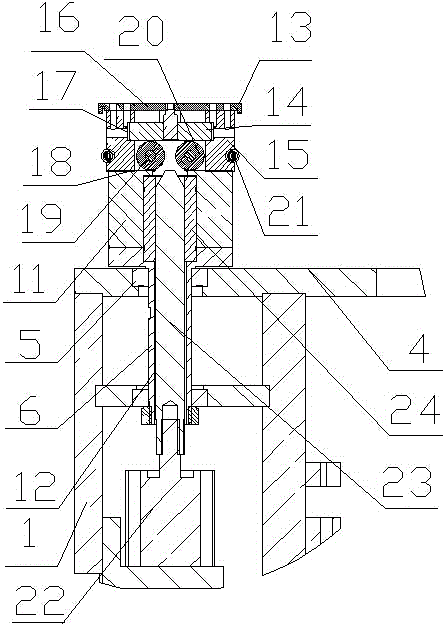
[0011] Such as figure 1 , 2 As shown, the present invention includes a bracket 1 , a steering mechanism 2 and a positioning mechanism 3 .

[0012] The steering mechanism 2 includes a bearing seat 4 fixed on the upper end of the bracket 1. A vertically arranged rotating shaft 6 is installed on the bearing seat 4 through a first bearing 5. The upper end of the rotating shaft 6 protrudes upwards from the bearing seat 4. One part of the rotating shaft 6 A rotary motor 7 is installed on the side, the output end of the rotary motor 7 is connected with a first pulley 8, and the rotary shaft 6 is fixed with a second pulley 9, and the first pulley 8 and the second pulley 9 are connected through a belt 10 transmission.

[0013] The positioning mechanism 3 includes a fixed seat 11, the fixed seat 11 is fixed on the upper end of the rotating shaft 6, the fixed seat 11 and the rotating shaft 6 are all provided with an axial center through hole 12, and the upper end of the fixed seat 11 is...


PUM


Abstract

A semiconductor element positioning and turning device relates to the field of semiconductor element processing. The semiconductor element positioning and turning device comprises a bracket, a turning mechanism and a positioning mechanism, wherein the turning mechanism comprises a bearing block fixed at the upper end of the bracket; a vertically arranged rotating shaft is mounted on the bearing block through a first bearing; the upper end of the rotating shaft extends up out of the bearing block; a rotating motor is mounted on one side of the rotating shaft; the rotating motor is in transmission connection with the rotating shaft through a belt; the positioning mechanism comprises a fixed seat; the fixed seat is fixed at the upper end of the rotating shaft; axial central through holes are formed in the fixed seat and the rotating shaft; and a four-jaw chuck is fixed at the upper end of the fixed seat. The semiconductor element positioning and turning device simplifies the structure of a conventional semiconductor element sorting, marking and taping integrated machine, reduces the cost and improves the production efficiency.

Description

technical field [0001] The invention relates to the field of semiconductor element processing, in particular to a semiconductor element positioning and steering device. Background technique [0002] In the production process of semiconductor components, the direction of semiconductor components needs to be corrected before many processes. The correction work is divided into two steps of positioning and steering to realize the calibration of semiconductor components; in the prior art, the positioning and steering of semiconductor components are carried out through It is realized by two sets of devices and two processes, resulting in a relatively complicated structure of the equipment and low work efficiency. Contents of the invention [0003] The object of the present invention is to provide a positioning and steering device for semiconductor elements that can realize positioning and steering in one. [0004] The semiconductor element positioning steering device includes a...

Claims


Application Information

Patent Timeline
Patent Type & Authority Applications(China)
IPC IPC(8): B65G47/244B65G47/88
Inventor 李永备胡志川张磊
Owner 扬州泽旭电子科技有限责任公司
Learn More