Processing and positioning component for pcb

A technology for positioning components and pcb boards, which is applied in the direction of PCB positioning, electrical components, and assembling printed circuits with electrical components during processing, which can solve the problem that mobile phone PCB boards cannot be processed in batches.

Inactive Publication Date: 2016-05-11
TIANJIN HUAMAI TECH
View PDF4 Cites 3 Cited by
  • Summary
  • Abstract
  • Description
  • Claims
  • Application Information

AI Technical Summary

Problems solved by technology

[0005] The technical problem to be solved by the present invention is: in order to solve the problems existing in the above-mentioned background technology, a k

Method used


Image

  • Processing and positioning component for pcb
  • Processing and positioning component for pcb

Examples


Embodiment 1

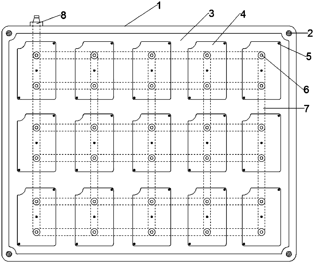
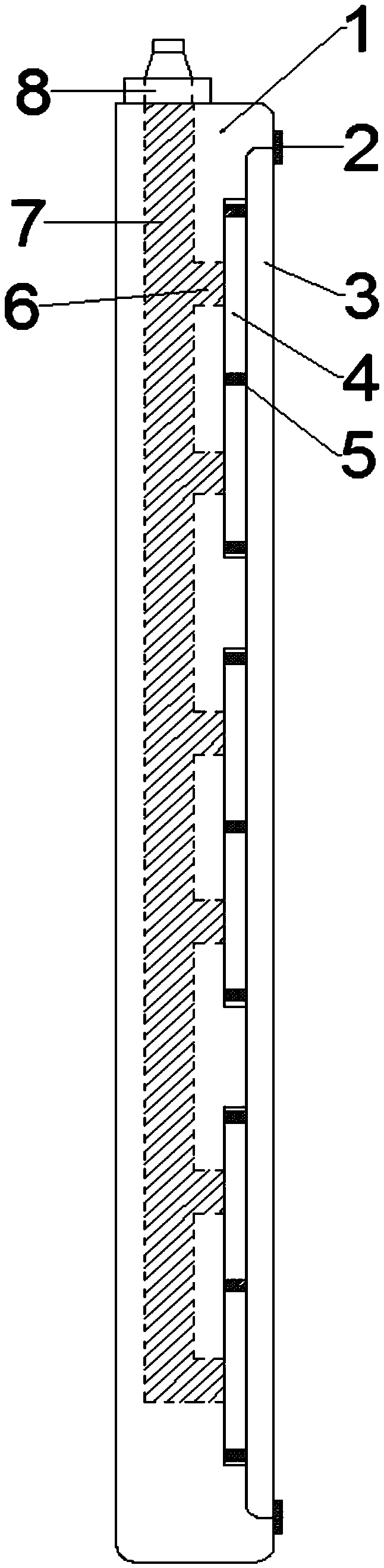
[0020] Embodiment 1: When the actual carrier tray is used, a pcb board processing and positioning assembly includes a tray body 1, the upper surface of the tray body 1 is rectangular, and the four corners of the tray body 1 are respectively fixed with a tray positioning device 2, and the tray body 1 The upper surface is fixedly provided with a feeding trough 3, and the lower surface of the feeding chute 3 is fixedly provided with a plurality of mounting holes 4, and the surface of the mounting hole 4 is fixedly provided with a plurality of fixing bolts 5, and the surface of the mounting hole 4 is fixedly provided with a plurality of fixing holes 6, The inside of the tray body 1 is fixedly provided with an air channel 7 corresponding to the fixing hole 6 , and the side of the tray body 1 is fixedly provided with an air suction port 8 .

[0021] As a preferred solution, the number of 5 fixing bolts in each mounting hole 4 is three; as a preferred solution, the number of 6 fixing ...

Embodiment 2

[0023] Embodiment 2: After using the carrier tray, a pcb board processing and positioning assembly includes a tray body 1, the upper surface of the tray body 1 is rectangular, and the four corners of the tray body 1 are respectively fixed with tray positioning devices 2, and the upper surface of the tray body 1 The surface is fixed with a feed trough 3, the lower surface of the feed trough 3 is fixed with a plurality of installation holes 4, the surface of the installation hole 4 is fixed with a plurality of fixing bolts 5, the surface of the installation hole 4 is fixed with a plurality of fixing holes 6, the tray The inside of the main body 1 is fixedly provided with an air passage 7 corresponding to the fixing hole 6 , and the side of the tray main body 1 is fixedly provided with an air suction port 8 .

[0024] As a preferred solution, the number of 5 fixing bolts in each mounting hole 4 is three; as a preferred solution, the number of 6 fixing holes in each mounting hole 4...


PUM


Abstract

The invention relates to the technical field of carrier devices, and particularly provides a processing and positioning component for a pcb. The processing and positioning component for the pcb comprises a tray body. The four corners of the tray body are fixedly provided with a tray positioning device respectively. A material feeding groove is fixedly arranged on the upper surface of the tray body. Plural installing holes are fixedly arranged on the lower surface of the material feeding groove. Plural fixing bolts are fixedly arranged on the surface of the installing holes. Plural fixing holes are fixedly arranged on the surface of the installing holes. The internal part of the tray body is provided with air channels which are fixedly arranged in a way of being corresponding to the fixing holes. The side surface of the tray body is fixedly provided with an air suction port. Accurate positioning of the tray body on an SMT machine can be realized by arrangement of the positioning devices, accurate positioning of a mobile phone PCB on the tray body can be realized by arrangement of the installing holes and the fixing bolts, and the function of fixing the mobile phone PCB through negative pressure can be realized by arrangement of the fixing holes, the air channels and the air inlet so that accurate positioning and processing of the mobile phone PCB can be realized in batches.

Description

technical field [0001] The invention relates to the technical field of carrier devices, in particular to a pcb board processing and positioning assembly. Background technique [0002] The Chinese name of PCB is "printed circuit board", also known as printed circuit board and printed circuit board. It is an important electronic component, a support for electronic components, and a provider of electrical connections for electronic components. Because it is produced using electronic printing technology (ie SMT), it is called a "printed" circuit board. [0003] The electronics industry is constantly evolving as people's demand for electronics, especially mobile phones, is becoming more and more common. As an important SMT (Surface Mount Technology, SMT) in the production of mobile phone PCB boards, it is called surface mount or surface mount technology. It is a method of mounting non-pin or short lead surface mount components on printed circuit boards On the surface of the cir...

Claims


Application Information

Patent Timeline
IPC IPC(8): H05K3/30
CPCH05K3/303H05K2203/15
Inventor 马玉刚
Owner TIANJIN HUAMAI TECH
Why Eureka
Try Eureka