An automatic optical detection device and detection method thereof

An automatic optical inspection and component technology, which is applied in the direction of optical testing defects/defects, etc., can solve the problems that are difficult to adapt to dense and fine-pitch board testing tasks, uneconomical, and time-consuming

Active Publication Date: 2018-11-16
SUZHOU MINGFU AUTOMATIC SCI & TECH
View PDF7 Cites 0 Cited by
  • Summary
  • Abstract
  • Description
  • Claims
  • Application Information

AI Technical Summary

Problems solved by technology

[0002]With the advancement of production technology, PCB board or firmware is becoming more and more complex, traditional in-circuit test lCT and functional test are becoming laborious and time-consuming
It is difficult to adapt to the test tasks of dense and fine-pitch boards by using the bed of needles test
For high-density and complex surface-mount PCBs, manual visual inspection is neither reliable nor economical, and for tiny components such as 0402, 0201, etc., manual visual inspection has actually lost its meaning

Method used


Image

  • An automatic optical detection device and detection method thereof
  • An automatic optical detection device and detection method thereof
  • An automatic optical detection device and detection method thereof

Examples


Embodiment Construction

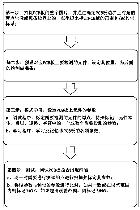
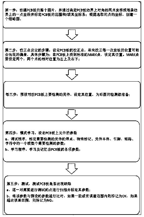
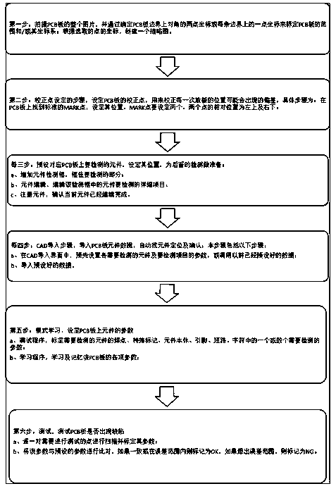
[0068] Hereinafter, the present invention will be described in detail with reference to the drawings and examples. It should be noted that, in the case of no conflict, the embodiments in the present application and the features in the embodiments can be combined with each other.

[0069] An automatic optical detection method provided by the present invention, some embodiments of which are as follows figure 1 shown, including the following steps:

[0070] Step 1: Take the entire picture of the PCB board, and demarcate the scope of the PCB board and / or its coordinate system by determining the coordinates of two points on the opposite corners of the PCB board boundary or one point on each boundary; Each point of the point leads to two straight lines perpendicular to each other, and these four straight lines intersect to form a rectangle, which is consistent with the size and shape of the PCB board. Similarly, if any point is selected on the four boundaries of the PCB board, the...


PUM


Abstract

The present invention provides an automatic optical detection apparatus for PCB board production, and a detection method thereof. According to the present invention, image acquisition is performed, the ranges of placed PCB boards to be detected each time are determined (the points on the boundaries of PCB board images are led out to obtain mutually perpendicular straight lines, the straight lines intersect to delineate a rectangular frame, and the size of the rectangular frame is corresponding to the size of the PCB board), the elements to be detected, the item contents to be detected and the qualified thresholds to be detected thereof on the PCB board having the model are edited, the values are preset in equipment, the values can be directly called if the values of the PCB board having the model are preset, the contents to be detected are studied and the detection path to be detected is optimized and determined before the detection, and finally detection comparison in a one-by-one manner is performed. The technical scheme of the present invention is simple and reliable, and has high efficiency.

Description

technical field [0001] The invention belongs to the field of automatic quality detection, in particular to an automatic optical detection device and a detection method for PCB board production. Background technique [0002] With the progress of the production process, the PCB board or firmware is becoming more and more complex, and the traditional in-circuit test lCT and functional test are becoming laborious and time-consuming. It is difficult to adapt to the test tasks of dense and fine-pitch boards by using the bed of needles test. For high-density and complex surface mount PCBs, manual visual inspection is neither reliable nor economical, and for tiny components such as 0402, 0201, etc., manual visual inspection has actually lost its meaning. Therefore, there is a need for an AOI auxiliary test method and device to overcome the above problems. As a beneficial supplement to ICT and functional testing, it can help manufacturers improve the pass rate of in-line testing (IC...

Claims


Application Information

Patent Timeline
IPC IPC(8): G01N21/95
Inventor 庄春明
Owner SUZHOU MINGFU AUTOMATIC SCI & TECH
Why Eureka
Try Eureka