Well resistor structure and manufacturing method thereof and silicon device on insulator

A manufacturing method and well resistance technology, which is applied in the manufacture of semiconductor devices, electrical components, semiconductor/solid-state devices, etc., can solve the problems of large lateral diffusion and difficulty in obtaining resistance, etc.

Inactive Publication Date: 2016-03-30
CSMC TECH FAB2 CO LTD
View PDF7 Cites 4 Cited by
  • Summary
  • Abstract
  • Description
  • Claims
  • Application Information

AI Technical Summary

Problems solved by technology

This is because the lateral diffusion of the well is relatively large, so it is difficult to obtain a more accurate resistance under the same device area.

Method used


Image

  • Well resistor structure and manufacturing method thereof and silicon device on insulator
  • Well resistor structure and manufacturing method thereof and silicon device on insulator
  • Well resistor structure and manufacturing method thereof and silicon device on insulator

Examples


Embodiment Construction

[0022] In order to make the objects, features and advantages of the present invention more comprehensible, specific implementations of the present invention will be described in detail below in conjunction with the accompanying drawings.

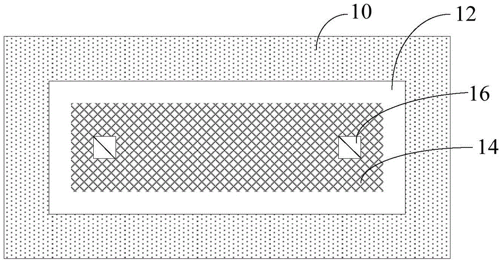
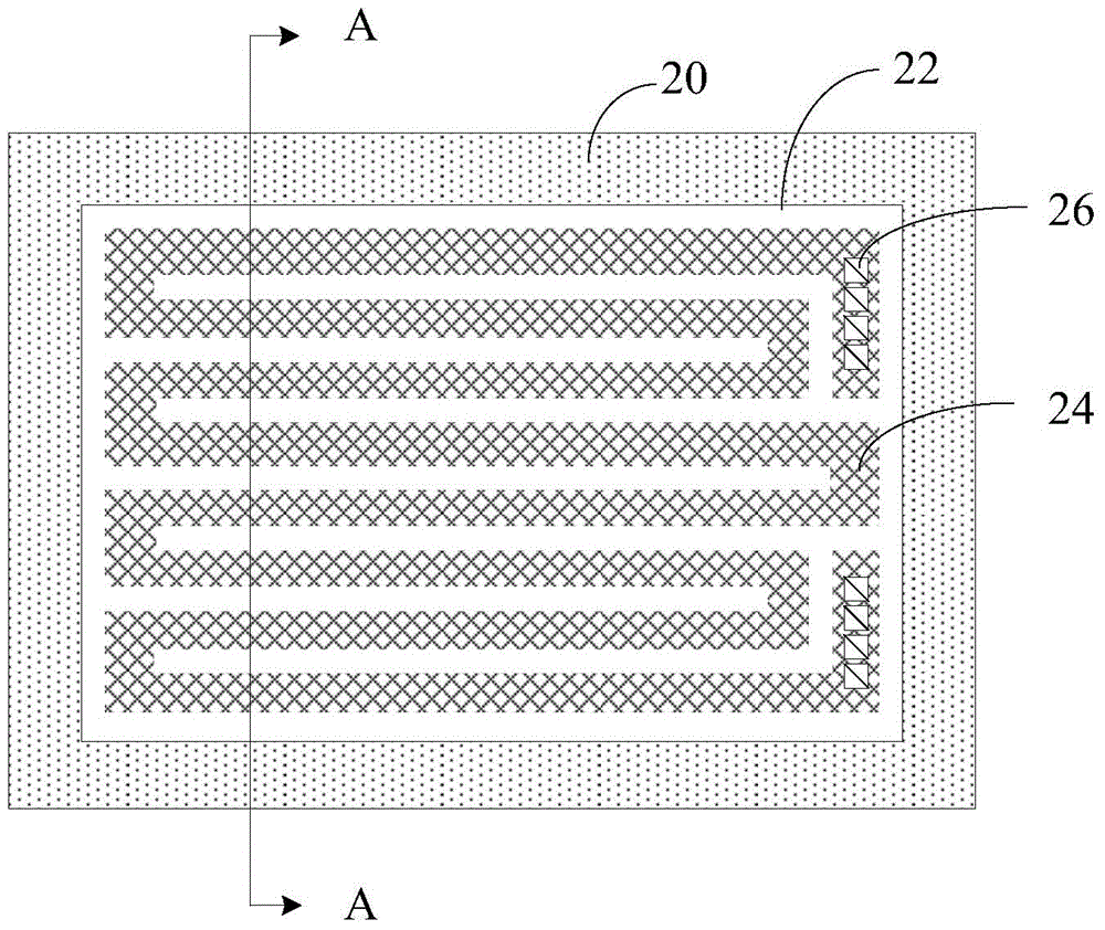
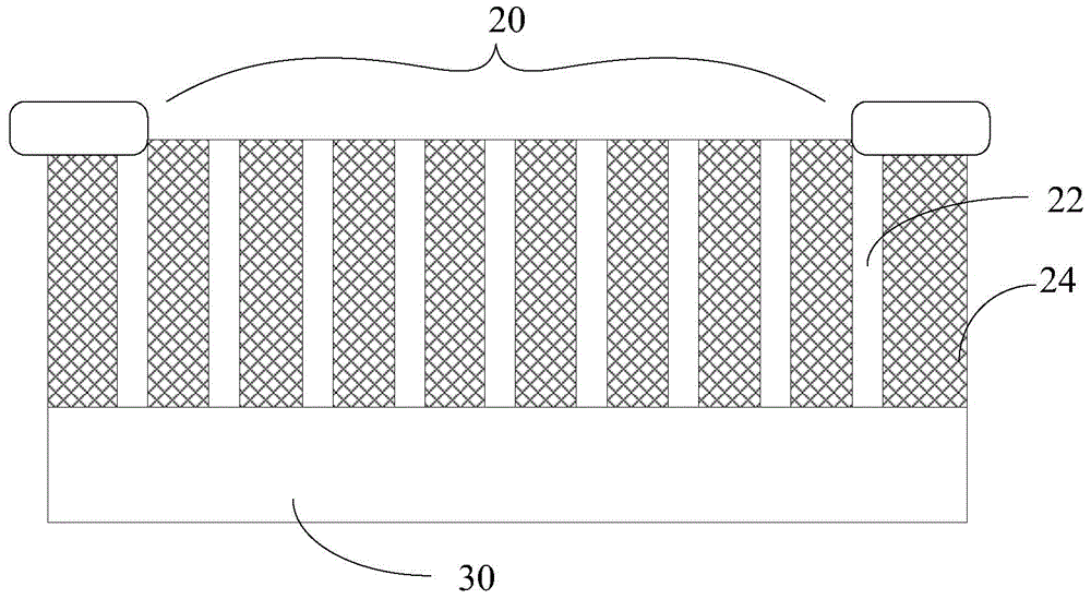
[0023] figure 1 It is a top view of the well resistor structure in an embodiment. Including insulation ( figure 1 not shown) and the active region 10 on the insulating layer. The active region 10 includes a well region 14 and a trench isolation structure 12 extending down to the insulating layer. The trench isolation structure 12 surrounds the well region 14 laterally and separates the well region 14 vertically. That is to say, the depth of the trench isolation structure 12 must be at least the same as that of the well region 14 , so that the well region 14 cannot extend laterally beyond the trench isolation structure 12 at the position where the trench isolation structure 12 is disposed. The cross section of the well region 14 is elonga...


PUM


Abstract

The invention relates to a well resistor structure, including an insulating layer and an active region on the insulating layer. The active region includes a well region, and also includes a trench isolation structure extending downwards to the insulating layer, and the trench isolation structure surrounds the well region in a transverse direction and separates the well region in a vertical direction; and the well resistor structure also includes a metal contact which is arranged on the well region and is in contact with the well region. The invention also relates to a manufacturing method of the well resistor structure and a silicon device on an insulator. According to the well resistor structure provided by the invention, the trench isolation structure is formed in the active region, so that the well region is blocked by the trench isolation structure in the transverse direction, transverse diffusion of majority carriers is not formed, and thus well resistance with a relatively accurate resistance value can be obtained.

Description

technical field [0001] The invention relates to a semiconductor device, in particular to a well resistance structure, a manufacturing method of the well resistance structure, and a silicon-on-insulator device including the well resistance structure. Background technique [0002] In analog circuit design, the error of resistance is generally divided into absolute error and matching error. In general, the absolute error of the device will be much larger than the matching error of the device. Because the absolute error of the resistor is relatively large, generally resistors are used in circuits that require very low absolute error, and the matching accuracy of the resistors is generally considered in circuit design. For matching accuracy, poly resistors are generally better than well resistors. This is because the lateral diffusion of the well is relatively large, so it is difficult to obtain a relatively accurate resistance under the same device area. Therefore, polycrysta...

Claims


Application Information

Patent Timeline
IPC IPC(8): H01L29/76H01L21/334
Inventor 王蛟宋华杨欢
Owner CSMC TECH FAB2 CO LTD
Why Eureka
Try Eureka