Micro-light-emitting diode

A light-emitting diode and miniature technology, which is applied in the direction of electrical components, circuits, semiconductor devices, etc., can solve the problems of drop, instability, and drop in tolerance value of changes, and achieve low side surface leakage current, increased current density, and low electrostatic sensitivity. Effect

Active Publication Date: 2016-02-24
MIKRO MESA TECH
View PDF5 Cites 2 Cited by
  • Summary
  • Abstract
  • Description
  • Claims
  • Application Information

AI Technical Summary

Problems solved by technology

The energy generated by this non-radiative recombination will replace light energy with heat energy, and greatly reduce the luminous efficiency of light-emitting diodes.
In addition, as the size of LEDs tends to be miniaturized, the problem caused by this phenomenon will become more serious because electrons and holes will more easily diffuse to the side surfaces of the miniature LEDs
[0004] Besides, since electrons and holes will diffuse more easily onto the side surfaces of the MLED, the current density in the light-emitting region of the MLED will decrease and become unstable.
In the light-emitting area of ​​the micro-LED, this decreased and unstable current density will also lead to a decrease in the luminous efficiency of the micro-LED
[0005] Furthermore, generally speaking, there will be a large number of lattice defects on the side surface of the light emitting diode due to the etching and / or cutting process, and these lattice defects will lead to the generation of leakage current
When the size of light-emitting diodes is miniaturized, the proportion of lattice defects in micro-light-emitting diodes will increase, which will increase the proportion of leakage current to the total current in micro-light-emitting diodes, and lead to a decrease in the luminous efficiency of micro-light-emitting diodes
[0006] In addition, when the size of light-emitting diodes is miniaturized, the process variation tolerance of micro-light-emitting diodes decreases, and therefore the yield rate of micro-light-emitting diodes also decreases.

Method used


Image

  • Micro-light-emitting diode
  • Micro-light-emitting diode
  • Micro-light-emitting diode

Examples


Embodiment Construction

[0045] A number of implementations of the present invention will be disclosed below with the accompanying drawings. For the sake of clarity, many specific details will be described together in the following description. It should be understood, however, that these specific details should not be used to limit the invention. That is, in some embodiments of the invention, these specific details are not necessary. In addition, for the sake of simplification of the drawings, some conventional structures and elements will be shown in a simple and schematic manner in the drawings.

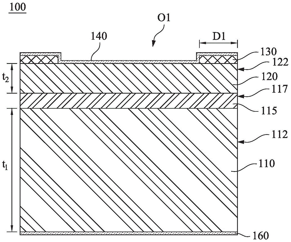
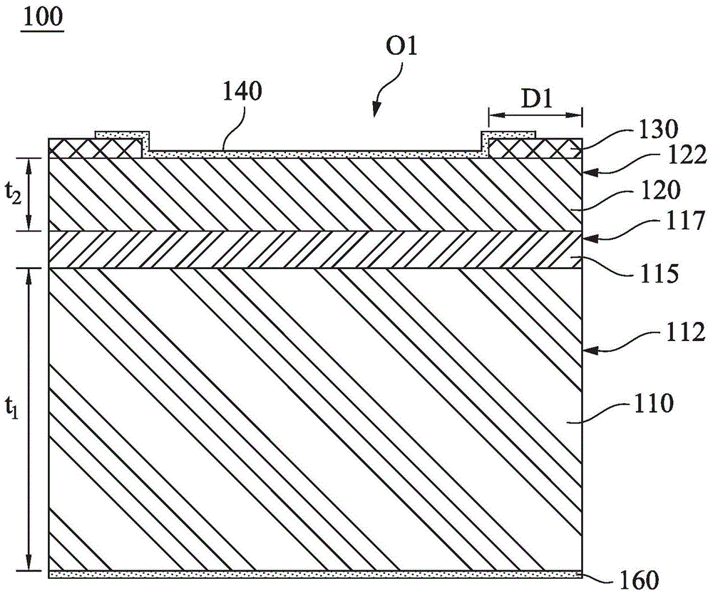
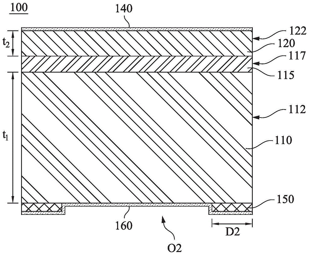
[0046] figure 1 It is a side cross-sectional view of the micro LED 100 according to the first embodiment of the present invention. The micro LED 100 includes a first type semiconductor layer 110 , an active layer 115 , a second type semiconductor layer 120 , a first dielectric layer 130 and a first electrode 140 . The second-type semiconductor layer 120 is disposed on the first-type semiconductor layer...


PUM


Abstract

A micro-light-emitting diode (micro-LED) includes a first type semiconductor layer, a second type semiconductor, a first dielectric layer, and a first electrode. The second type semiconductor layer is disposed on or above the first type semiconductor layer. The first dielectric layer is disposed on the second type semiconductor layer. The first dielectric layer has at least one opening therein to expose at least one part of the second type semiconductor layer. A first shortest distance between an edge of the opening of the first dielectric layer and a side surface of the second type semiconductor layer is greater than or equal to 1 [mu]m. The first electrode is partially disposed on the first dielectric layer and is electrically coupled with the exposed part of the second type semiconductor layer through the opening of the first dielectric layer. Since the first shortest distance is greater than or equal to 1 [mu]m, the number of electric carriers diffused to the side surface of the micro-LED is very few or nearly zero so that the light-emitting efficiency of the micro-LED is increased.

Description

technical field [0001] The invention relates to a miniature light-emitting diode. Background technique [0002] In recent years, light-emitting-diodes (light-emitting-diodes; LEDs) have been widely used in general lighting and commercial lighting applications. When used as a light source, LEDs have many advantages such as lower power consumption, longer lifetime, smaller size and faster switching. Therefore, traditional lighting, such as incandescent light sources, has been gradually replaced by LED light sources. [0003] In light-emitting diodes, when electrons and holes recombine in the energy gap of the semiconductor, the energy generated by the recombination will be released in the form of photons, and light will be generated. This recombination mechanism is called radiative recombination. However, when electrons and holes recombine in the defect energy gap of the semiconductor, the energy generated by the recombination will be released in the form of heat instead of...

Claims


Application Information

Patent Timeline
Patent Type & Authority Applications(China)
IPC IPC(8): H01L33/02
CPCH01L33/02H01L33/38H01L33/44
Inventor 张珮瑜
Owner MIKRO MESA TECH
Why Eureka
Try Eureka