Conductive film

A technology of conductive film and conductive area, applied in the field of electronics, can solve the problems of different light transmittance between insulating area and isolation area, affecting the overall appearance of conductive film, etc., to improve the uniformity of light transmission and improve the visual effect.

Inactive Publication Date: 2016-02-17
SHENZHEN O FILM TECH +2
View PDF6 Cites 0 Cited by
  • Summary
  • Abstract
  • Description
  • Claims
  • Application Information

AI Technical Summary

Problems solved by technology

It can be seen that in the prior art, the light transmittance between the conductive region, the insulating region and the isolation region is still slightly different, which affects the overall appearance of the conductive film.

Method used


Image

  • Conductive film
  • Conductive film
  • Conductive film

Examples


Embodiment Construction

[0024] The technical solutions in the embodiments of the present invention will be clearly and completely described below in conjunction with the accompanying drawings in the embodiments of the present invention. Obviously, the described embodiments are part of the embodiments of the present invention, rather than all of them. Based on the embodiments of the present invention, all other embodiments obtained by those of ordinary skill in the art without creative work shall fall within the protection scope of the present invention.

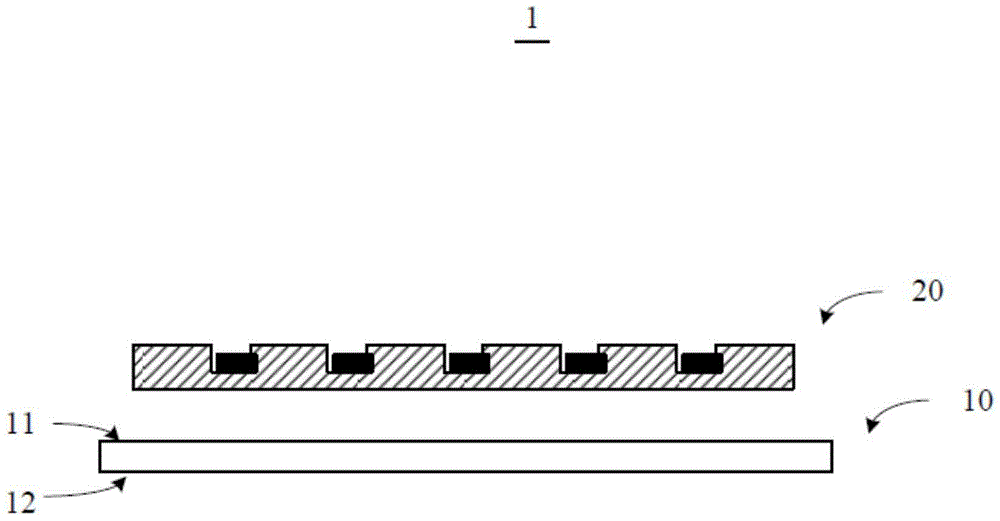
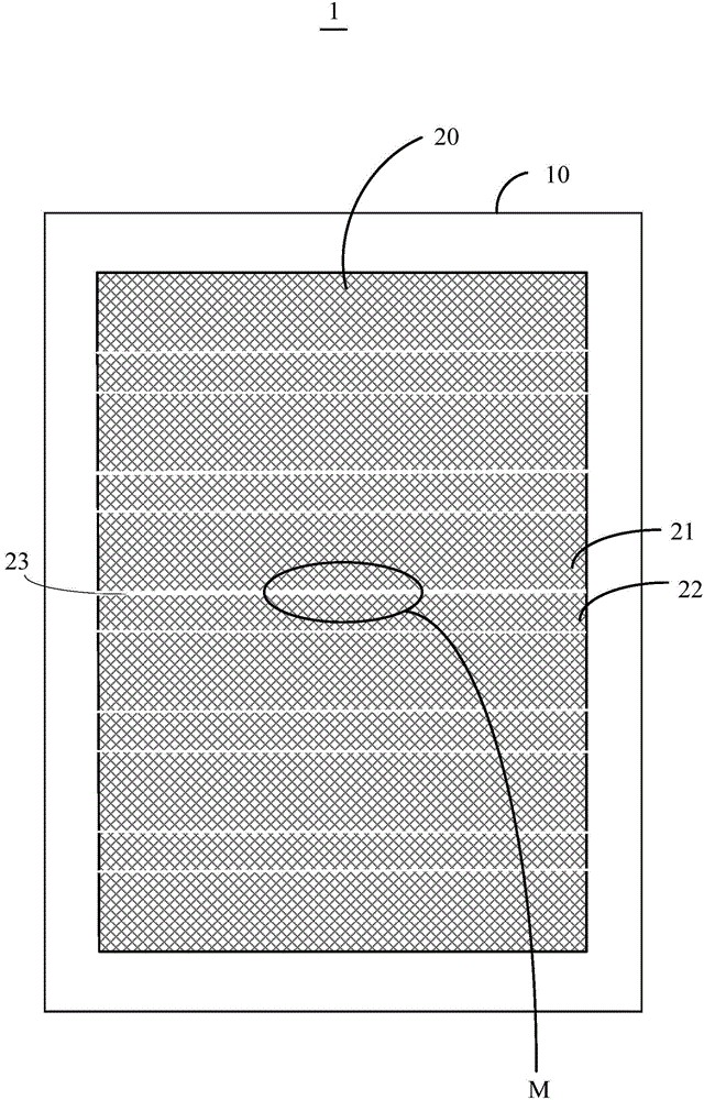
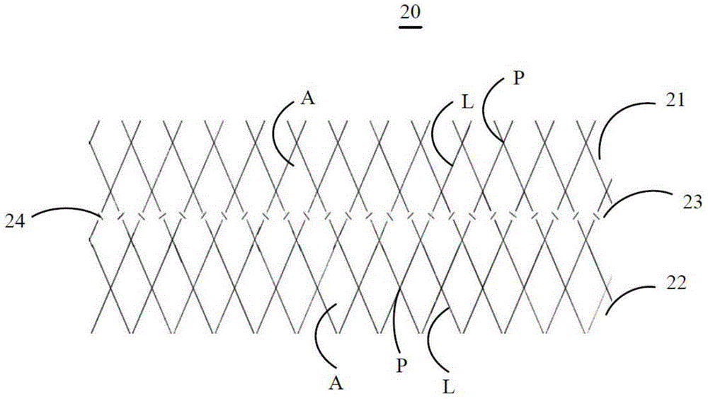
[0025] Please refer to figure 1 , figure 2 and image 3 , figure 1 It is a three-dimensional exploded schematic diagram of the conductive film provided by the first embodiment of the present invention. figure 2 It is a schematic diagram of the planar structure of the conductive film provided by the first embodiment of the present invention. image 3 for figure 2 Enlarged view of M shown. The conductive film 1 includes a substrate 10 and a transparent...


PUM


Abstract

The invention provides a conductive film. The conductive film comprises a substrate and a transparent conductive layer, wherein the substrate comprises a first surface and a second surface opposite to the first surface; the transparent conductive layer is arranged on the first surface or the first surface and the second surface and comprises multiple conductive areas and multiple insulation areas, the multiple conductive areas and the multiple insulation areas are formed by conductive materials configured to be grids, and the grids comprise multiple nodes and multiple grid lines connecting the multiple nodes; the conductive areas and the insulation areas are extended along a first direction and are arranged at intervals in a second direction orthogonal to the first direction so as to form a first gap between the conductive areas and the insulation areas which are adjacent to each other; and the transparent conductive layer further comprises a first auxiliary line which is arranged at the first gap and does not communicate with the first gap. The light transmittance distribution of the conductive film is quite uniform.

Description

Technical field [0001] The present invention relates to the field of electronic technology, in particular to a conductive film. Background technique [0002] The conductive film is a kind of conductive film with good conductivity and high light transmittance in the visible light band. At present, conductive films have been widely used in flat panel displays, photovoltaic devices, touch sensors, electromagnetic shielding and other fields, and have an extremely broad market space. The material for preparing the conductive film is generally indium tin oxide (Indium Tin Oxide, ITO), but in most practical applications such as touch screens, the preparation of the conductive film requires patterning of ITO to form a fixed conductive area and an insulating area on the surface of the substrate. . However, the patterning process of ITO often requires multiple processes such as exposure, imaging, etching, and cleaning, and the preparation process is more complicated. [0003] In compariso...

Claims


Application Information

Patent Timeline
Patent Type & Authority Applications(China)
IPC IPC(8): H01B5/14
Inventor 李默
Owner SHENZHEN O FILM TECH
Why Eureka
Try Eureka