A multi-band crystal spectrometer and its adjustment method
A crystal spectrometer and multi-band technology, applied in the field of multi-band crystal spectrometer and its adjustment, can solve the unfavorable design and arrangement of large-scale comprehensive experimental optical paths, affect the accuracy and stability of aiming, and take time to install and remove the needle tip, etc. , to achieve good overall optical density, avoid scattered light interference, and high aiming reliability
- Summary
- Abstract
- Description
- Claims
- Application Information
AI Technical Summary
Problems solved by technology
Method used
Image
Examples
Embodiment 1
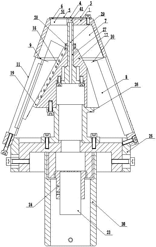
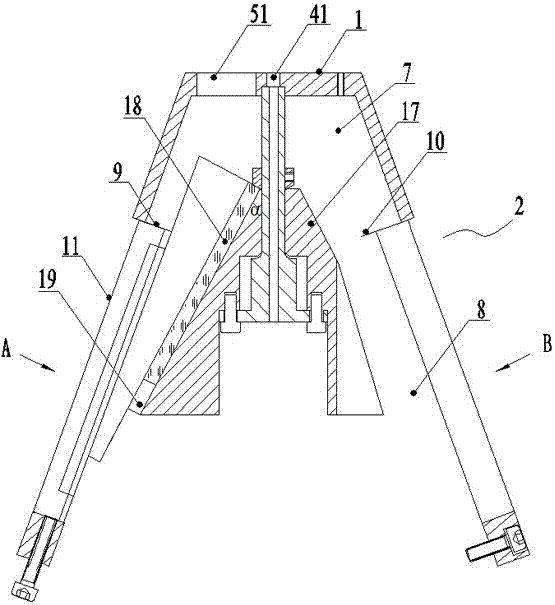
[0044] Such as Figure 2-Figure 12 , the multi-band crystal spectrometer of this embodiment includes a crystal spectroscopic system, a laser-assisted aiming system and a target room cantilever adjustment system;
[0045] The crystal light splitting system includes a hollow truncated conical shell 2 provided with an upper bottom surface 1, the upper bottom surface 1 is provided with a slit plate 3, and the center of the slit plate 3 is provided with a slit plate through hole 4, A slit 5 is radially provided on the slit plate 3, and a metal filter 6 is provided on the back of the slit 5, and the metal filter 6 completely covers the corresponding slit 5, and an upper bottom surface 1 is provided with Bottom surface through hole 41 and upper bottom surface slit 51, described upper bottom surface through hole 41 communicates with slit plate through hole 4 and is arranged coaxially, and described upper bottom surface slit 51 is set correspondingly with slit 5; The hollow cone The c...
Embodiment 2
[0058] In this embodiment, the number of slits is 6, and the slits are evenly distributed on the slit plate, and the included angle between the central axes of adjacent slits is 60°, and the width of each slit is 0.8 mm. The diameter of the through hole of the slit plate is 1.0 mm; the angle α between the crystal base and the central axis in this embodiment is 25°; the bumps are bumps distributed at intervals.
[0059] Other technical schemes in this embodiment are all the same as in Embodiment 1.
Embodiment 3
[0061] The number of slits in this embodiment is 4, and the slits are evenly distributed on the slit plate, and the included angle between the central axes of adjacent slits is 90°, and the width of each slit is 1.2 mm. The diameter of the through hole of the slit plate is 1.0 mm; the angle α between the crystal base and the central axis in this embodiment is 30°; the bumps are bumps distributed at intervals.
[0062] Other technical schemes in this embodiment are all the same as in Embodiment 1.
PUM
| Property | Measurement | Unit |
|---|---|---|
| width | aaaaa | aaaaa |
| diameter | aaaaa | aaaaa |
Abstract
Description
Claims
Application Information
 - R&D
- Intellectual Property
- Life Sciences
- Materials
- Tech Scout
- Unparalleled Data Quality
- Higher Quality Content
- 60% Fewer Hallucinations
Browse by: Latest US Patents, China's latest patents, Technical Efficacy Thesaurus, Application Domain, Technology Topic, Popular Technical Reports.
© 2025 PatSnap. All rights reserved.Legal|Privacy policy|Modern Slavery Act Transparency Statement|Sitemap|About US| Contact US: help@patsnap.com


