A display substrate, manufacturing method thereof, and display device

A technology of a display substrate and a manufacturing method, which are applied in the fields of display devices, display substrates and manufacturing methods thereof, can solve the problems of uneven thickness of the display substrate box and the degradation of the picture display quality of the display device, so as to improve the picture display quality and prevent the box Thick uneven effect

Inactive Publication Date: 2018-02-13
BOE TECH GRP CO LTD +1
View PDF3 Cites 0 Cited by
  • Summary
  • Abstract
  • Description
  • Claims
  • Application Information

AI Technical Summary

Problems solved by technology

[0005] The object of the present invention is to provide a display substrate and its manufacturing method, and a display device, which is used to solve the problem of the uneven cell thickness of the display substrate caused by the uneven total thickness of the functional layers of the array substrate, which leads to the reduction of the picture display quality of the display device. technical problem

Method used


Image

  • A display substrate, manufacturing method thereof, and display device
  • A display substrate, manufacturing method thereof, and display device
  • A display substrate, manufacturing method thereof, and display device

Examples


Embodiment Construction

[0031] In order to further illustrate the display substrate, the manufacturing method thereof, and the display device provided by the embodiments of the present invention, a detailed description will be given below in conjunction with the accompanying drawings.

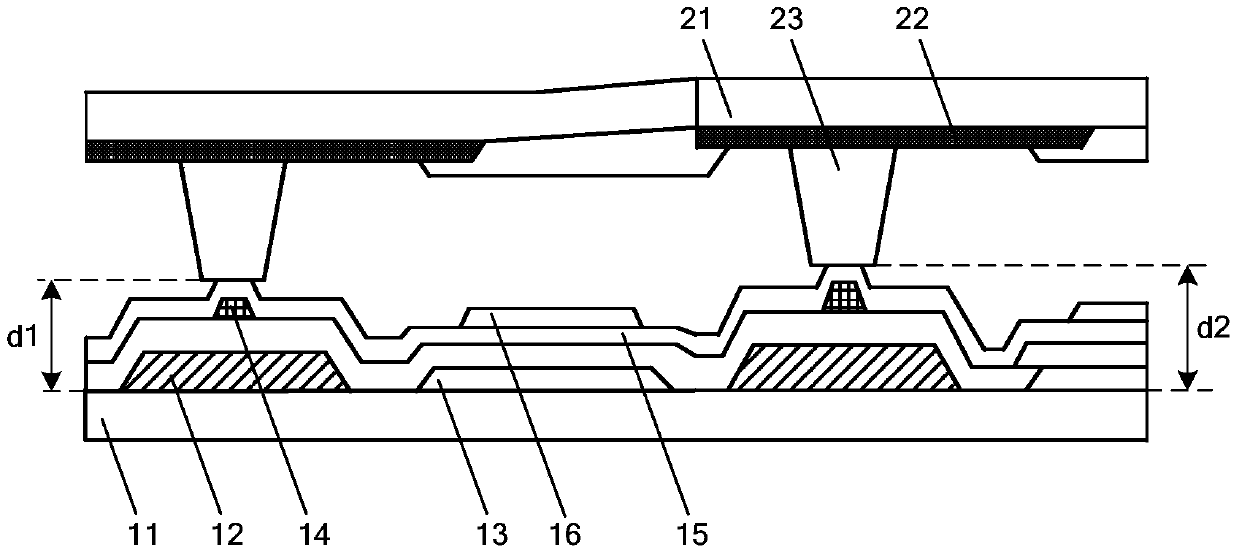
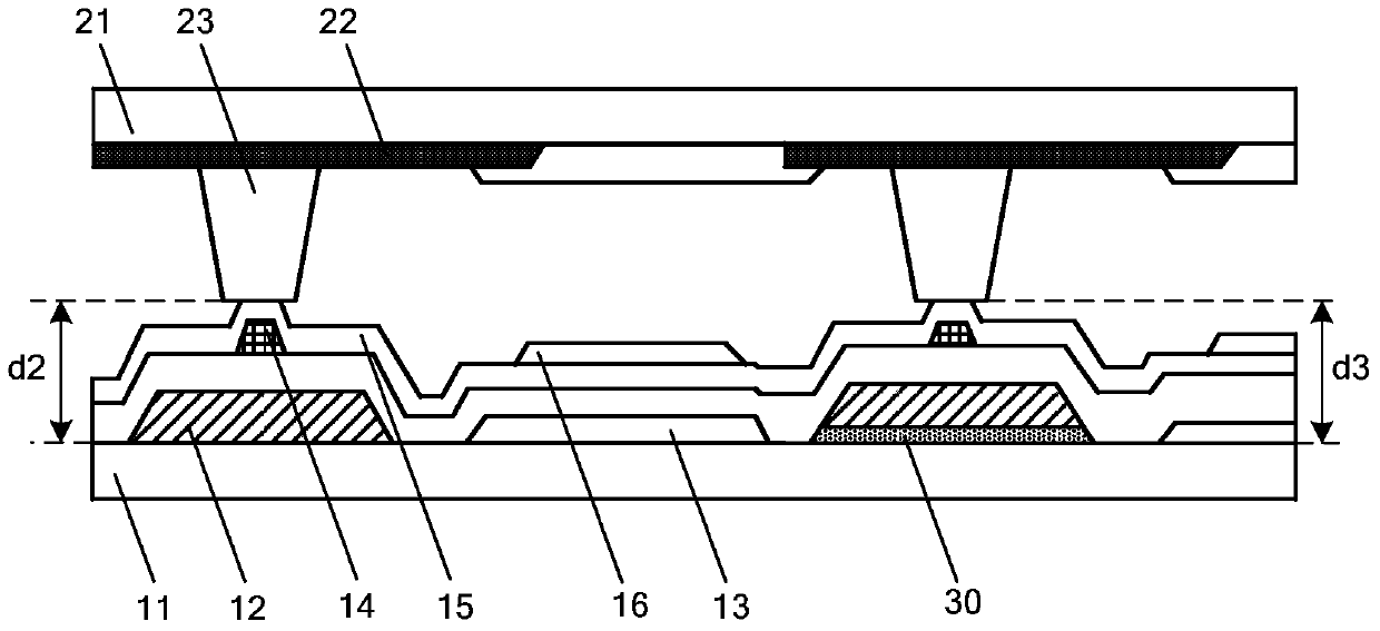
[0032] see figure 2 The display substrate provided by the embodiment of the present invention includes a first substrate 11 and a second substrate 21 oppositely arranged, the first substrate 11 includes a first region and a second region, and the functional layer on the first substrate 11 located in the first region The total thickness is thinner than the total thickness of the functional layers in the second region; a thickness compensation layer 30 is provided between the first substrate 11 and the second substrate 21, the thickness compensation layer 30 corresponds to the first region, and the thickness compensation layer 30 and The total thickness of the functional layers in the first region is equal to the total...


PUM


Abstract

The invention discloses a display substrate, a manufacturing method thereof, and a display device, and relates to the field of display technology, and aims to solve the problem that the picture display quality of the display device is lowered due to uneven cell thickness of the display substrate. The display substrate includes a first substrate and a second substrate oppositely arranged, the first substrate includes a first area and a second area, and the total thickness of the functional layers located in the first area on the first substrate is greater than that located in the second area. The total thickness of the functional layer is thin; a thickness compensation layer is provided between the first substrate and the second substrate, the thickness compensation layer corresponds to the first area, and the total thickness of the thickness compensation layer and the functional layer in the first area is the same as that of the second area The total thickness of the inner functional layer is equal. In the present invention, a thickness compensation layer corresponding to the first region is arranged between the first substrate and the second substrate, so that the cell thickness of each region of the display substrate is uniform, so as to improve the image display quality of the display device.

Description

technical field [0001] The invention relates to the field of display technology, in particular to a display substrate, a manufacturing method thereof, and a display device. Background technique [0002] Currently, the main structure of a display device includes a display substrate, such as figure 1 As shown, the display substrate includes a first substrate 11 and a second substrate 21 that are oppositely arranged; wherein, a plurality of functional layers are disposed on the first substrate 11 . When forming the functional layer on the first substrate 11, due to the influence of the manufacturing process, the total thickness of the functional layer is likely to be uneven. [0003] For example, when forming a metal functional layer such as a grid line layer on the first substrate 11, a metal thin film is first deposited on the first substrate 11 by magnetron sputtering, and then a grid line layer is formed through a patterning process. For the array substrate of a display d...

Claims


Application Information

Patent Timeline
Patent Type & Authority Patents(China)
IPC IPC(8): H01L27/12H01L21/77
CPCH01L21/77H01L27/12H10K59/131H10K50/8428H10K2102/351G02F1/136295G02F1/133512G02F1/133514G02F1/133516G02F1/13394G02F1/134309G02F1/136286G02F1/1368G02F2201/121G02F2201/123H01L27/124H01L27/1296
Inventor 蒋学兵张然高吉磊
Owner BOE TECH GRP CO LTD
Why Eureka
Try Eureka