Integrated packaging microwave device array parallel welding apparatus and method

A parallel welding, microwave device technology, applied in the direction of electric solid device, semiconductor device, semiconductor/solid state device manufacturing, etc., can solve the problems of bare chip damage, device solder remelting, limited use range and use efficiency, etc., to reduce labor Strength and operating time, avoid device damage, improve seam welding efficiency

Active Publication Date: 2015-10-07
CHINA ELECTRONIC TECH GRP CORP NO 38 RES INST
View PDF5 Cites 4 Cited by
  • Summary
  • Abstract
  • Description
  • Claims
  • Application Information

AI Technical Summary

Problems solved by technology

[0004] In order to solve this problem, in the parallel seam welding process, try to adopt the array solution commonly used in the previous process, try Figure 1 Complete the capping of multiple devices at one time, and face a new problem: the heat generated during the sequential capping of the devices arranged in an array spreads among each other, resulting in a rapid rise in the temperature of the devices, remelting of the solder inside the devices, and the glue A series of hidden dangers such as aging and bare chip failure
The development of integrated packaged microwave devices tends to install multiple bare chips in one device, because the large current generated during the parallel seam welding process will be introduced into the device through the pins, causing damage to the bare chips
The above problems greatly limit the application range and efficiency of parallel seam welding in the field of integrated packaging microwave device packaging, and limit the large-scale manufacturing of integrated packaging microwave devices

Method used


Image

  • Integrated packaging microwave device array parallel welding apparatus and method
  • Integrated packaging microwave device array parallel welding apparatus and method
  • Integrated packaging microwave device array parallel welding apparatus and method

Examples


Embodiment Construction

[0033] The embodiments of the present invention are described in detail below. This embodiment is implemented on the premise of the technical solution of the present invention, and detailed implementation methods and specific operating procedures are provided, but the protection scope of the present invention is not limited to the following implementation example.

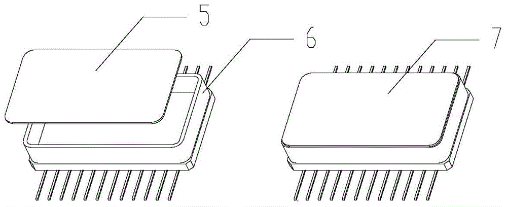
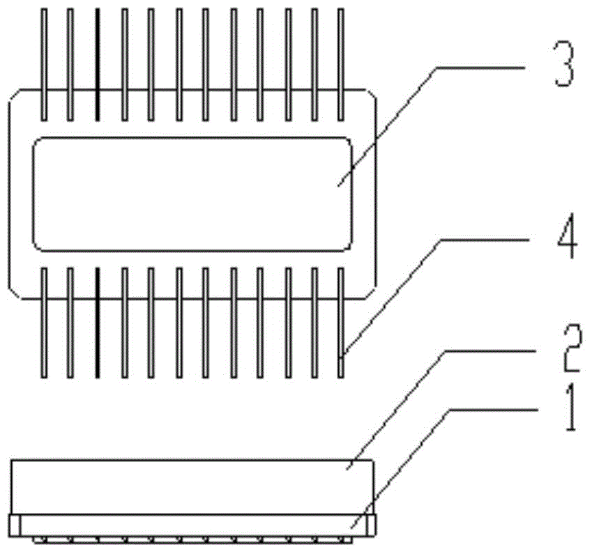
[0034] Such as Figure 1~3 As shown, the housing 6 for integrally packaging microwave devices includes a substrate 1 , a surrounding frame 2 , a bottom plate 3 , and pins 4 . Among them, there is a circuit pattern inside the substrate 1, and a bare chip is installed on the surface, and the electrical interconnection is realized by means of gold wire on the bare chip; The input and output of pin 4 are realized. The surrounding frame 2 and the bottom plate 3 are used to realize the sealing of the bottom and side of the device.

[0035] The casing 6 and the device cover 5 can be tightly connected by means of parall...


PUM


Abstract

The invention discloses an integrated packaging microwave device array parallel welding apparatus and method. The front side of a positioning clamp is provided with a plurality of welding chambers arranged in arrays; insulation heat dissipation substrates are welded in the welding chambers, and are level with the front side of the positioning clamp; a clamp cover plate is provided with a plurality of fixing through holes arranged in arrays; the fixing through holes match the frame dimension of a device to be welded; a clamp insulating layer covers the back side of the clamp cover plate; a cover plate insulating layer covers the front surface of the positioning clamp except the welding chambers. The apparatus and method can rapidly dissipate great heat generated in the array parallel welding process of an integrated packaging microwave device, and avoid the problems of device temperature rapid rising, device internal welding flux remelting, rubber aging and bare chip loss caused by heat diffusion in successive covering processes of array devices.

Description

technical field [0001] The invention relates to an electronic device sealing technology, in particular to an array-type parallel welding device and method for integrated packaging of microwave devices. Background technique [0002] With the development of modern radars towards arrays and multi-units, the demand for rapid, efficient, low-cost and large-scale batch manufacturing of microwave devices has become stronger. Manufacturing microwave devices through integrated packaging is a cutting-edge solution. After the pins are sealed and tightly connected with the ceramic substrate and the surrounding frame by welding, how to realize the complete sealing of the integrated packaging device through the fast and efficient sealing of the cover plate after the bare chip and other expensive precision components are installed The problems that need to be faced down. [0003] To achieve a sealed connection between the cover plate and the surrounding frame, the sealing method of parall...

Claims


Application Information

Patent Timeline
IPC IPC(8): H01L21/60
CPCH01L24/81H01L2224/81098H01L2224/8111
Inventor 宋夏邱颖霞林文海胡骏金家富
Owner CHINA ELECTRONIC TECH GRP CORP NO 38 RES INST
Why Eureka
Try Eureka