Electronic device

A technology for electronic devices and electronic components, which can be applied in directions such as the installation of support structures, and can solve problems such as failure to obtain, high optical axis parallelism, and large distance errors.

Active Publication Date: 2015-09-09
HTC CORP
View PDF3 Cites 5 Cited by
  • Summary
  • Abstract
  • Description
  • Claims
  • Application Information

AI Technical Summary

Problems solved by technology

Since an electronic device with dual cameras uses two cameras for triangulation to calculate the distance between the object and the camera, this type of electronic device has higher requirements for the parallelism of the optical axis. If the optical axis shifts, the calculated The larger the distance error will be, and the photographic effect that meets the requirements cannot be obtained.

Method used


Image

  • Electronic device
  • Electronic device
  • Electronic device

Examples


Embodiment Construction

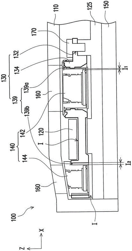
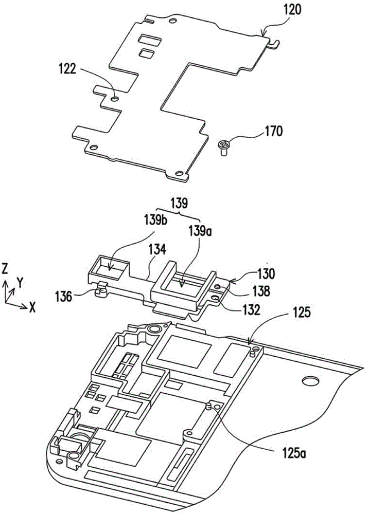
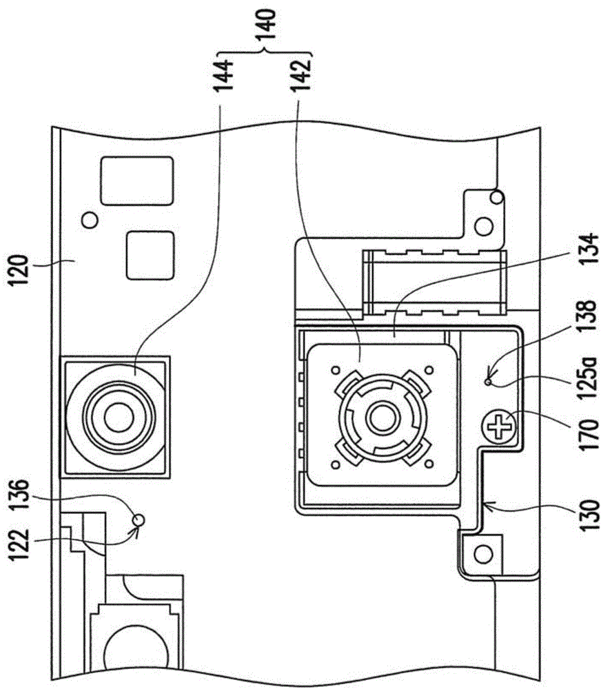
[0035] figure 1 is a partial cross-sectional schematic view of an electronic device according to an embodiment of the present invention. figure 2 Yes figure 1 Partially exploded schematic diagram of the electronic device. image 3 Yes figure 1 Partial schematic diagram of the electronic device with the back cover removed and the electronic components hidden. see Figure 1 to Figure 3 , the electronic device 100 of this embodiment includes a casing 110 , a circuit board 120 , a frame 125 , an electronic component support base 130 , a plurality of electronic components 140 , a screen 150 , a plurality of lenses 160 and screws 170 .

[0036] The circuit board 120 , the frame 125 , the electronic component support 130 and the electronic component 140 are located in the space of the housing 110 , the screen 150 is exposed from the housing 110 , and the lens 160 is penetrated through the housing 110 opposite to the screen 150 .

[0037] The electronic component support base 13...


PUM


Abstract

The invention discloses an electronic device, comprising a housing, a circuit board, a frame, an electronic member support base and a plurality of electronic member. The circuit board and the framework are arranged inside the housing. The electronic member support base is positioned inside the framework and comprises a fixing part and a bearing part. The fixing part is fixed to the framework as a support point of the support base of the electronic member. The electronic members are arranged on the circuit part and electrically coupled to the circuit board. Gaps are positioned between the bearing part and the framework and between the bearing part and the circuit board.

Description

technical field [0001] The present invention relates to an electronic device, and in particular to an electronic device with a lower probability of optical axis deviation. Background technique [0002] In recent years, with the development of the technology industry, electronic devices, such as smart phones or tablet computers, have frequently appeared in daily life. In addition to their own functions, these electronic devices are usually equipped with additional functional components to have additional functions. For example, an electronic device may be configured with components such as a camera. [0003] At present, the electronic device usually fixes the upper and lower sides of the camera through a fixing structure, and the surrounding side is limited by a chassis structure (chassis). However, when the electronic device is impacted, the optical axis of the camera will deviate along with the deformation of these fixed structures. With the advancement of technology, so...

Claims


Application Information

Patent Timeline
Patent Type & Authority Applications(China)
IPC IPC(8): H05K7/14
Inventor 陈易德刘韦承曾竣许嘉元赖仁正庄政洁孙金锴
Owner HTC CORP
Why Eureka
Try Eureka