Array substrate, fabricating method of array substrate, and display device

An array substrate and substrate substrate technology, which is applied in semiconductor/solid-state device manufacturing, instruments, organic semiconductor devices, etc., can solve the problems of increased product thickness, complex driving system, and increased production cost of double-sided display panels.

Active Publication Date: 2015-08-19
BOE TECH GRP CO LTD
View PDF4 Cites 14 Cited by
  • Summary
  • Abstract
  • Description
  • Claims
  • Application Information

AI Technical Summary

Problems solved by technology

However, the double-sided display panel in the prior art is actually a combination of two independent display panels. Its internal structure and the driving system for driving the two independent display panels to emit light are relatively complicated, which not only makes the production cost of the double-sided display panel Greatly improved, but also increases the thickness of the product, which does not conform to the trend of thinner and thinner display panels

Method used


Image

  • Array substrate, fabricating method of array substrate, and display device
  • Array substrate, fabricating method of array substrate, and display device
  • Array substrate, fabricating method of array substrate, and display device

Examples


Embodiment Construction

[0029] The following will clearly and completely describe the technical solutions in the embodiments of the present invention with reference to the accompanying drawings in the embodiments of the present invention. Obviously, the described embodiments are only some, not all, embodiments of the present invention. Based on the embodiments of the present invention, all other embodiments obtained by persons of ordinary skill in the art without making creative efforts belong to the protection scope of the present invention.

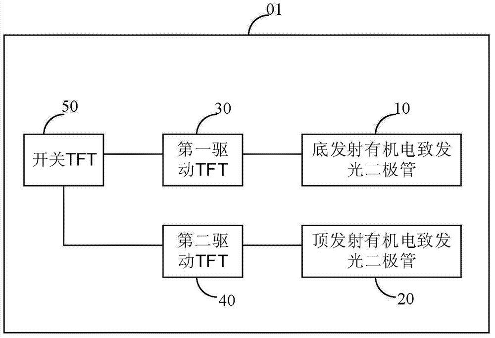
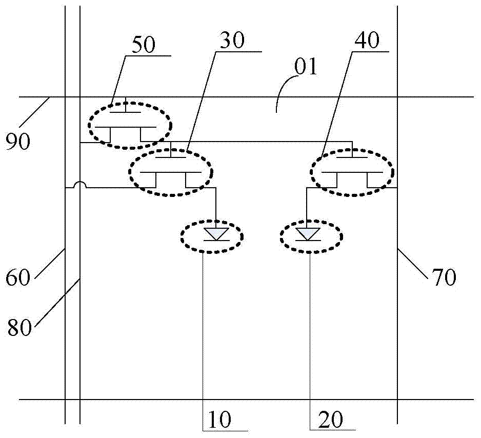
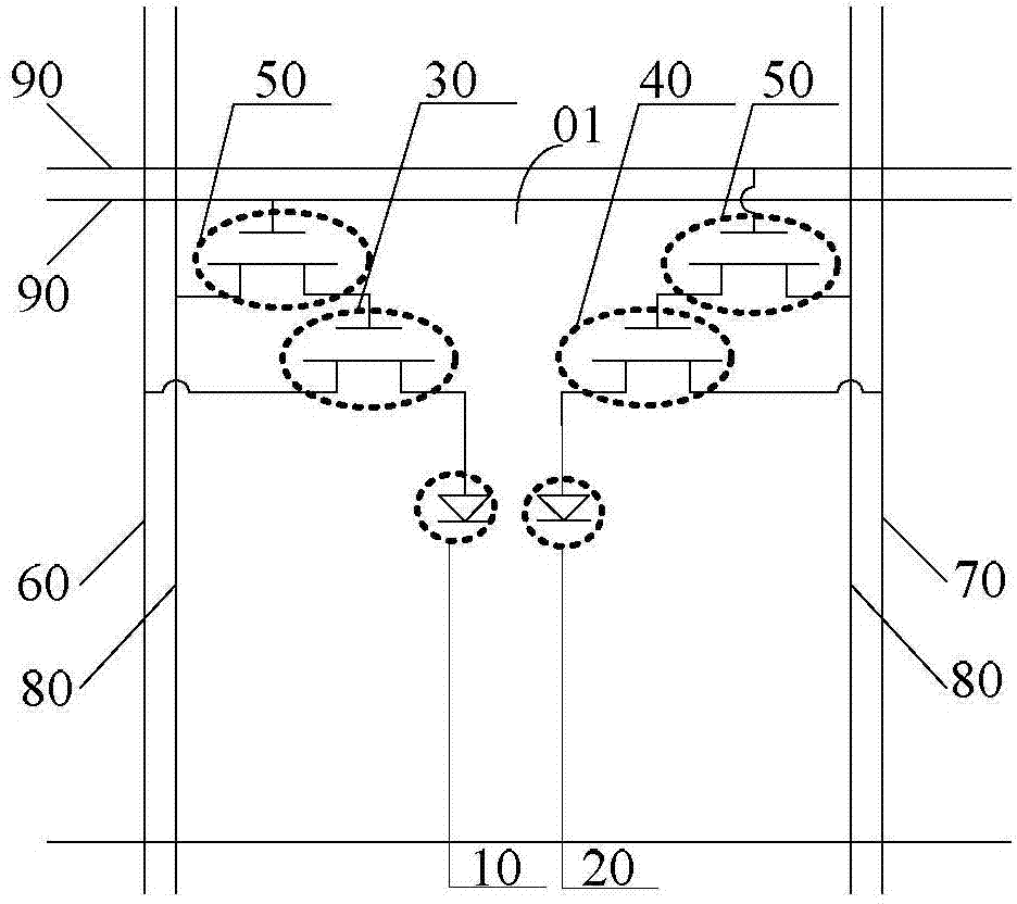
[0030] An embodiment of the present invention provides an array substrate, such as Figure 1-Figure 3 As shown, the array substrate includes a base substrate and a plurality of sub-pixel units 01 arranged in an array arranged on the same side of the base substrate, and each of the sub-pixel units 01 includes a bottom-emitting organic electroluminescent diode 10 , a top-emitting organic electroluminescent diode 20, a first drive TFT30, a second drive TFT40, and...


PUM


Abstract

The embodiment of the invention provides an array substrate, a fabricating method of the array substrate, and a display device, and relates to the technical field of displays. Dual-faced displaying can be realized. The array substrate comprises a plurality of sub-pixel units arranged in an array manner, wherein each sub-pixel unit comprises a bottom-emitting organic light emitting diode, a top-emitting organic light emitting diode, a first drive TFT, a second drive TFT and at least one switch TFT, wherein the at least one switch TFT is connected with the first drive TFT and the second drive TFT, and is used for controlling the starting of the first drive TFT and the second drive TFT; the first drive TFT is connected with the bottom-emitting organic light emitting diode and a first data line and is used for driving the bottom-emitting organic light emitting diode to emit light; the second drive TFT is connected with the top-emitting organic light emitting diode and a second data line and is used for driving the top-emitting organic light emitting diode to emit light. The array substrate is used in a dual-faced display type display device.

Description

technical field [0001] The present invention relates to the field of display technology, in particular to an array substrate, a preparation method thereof, and a display device. Background technique [0002] Organic Light Emitting Diode (OLED) display panels have the advantages of self-illumination, low power consumption, no viewing angle dead angle, fast response, high contrast, etc., and have strong competitiveness compared with liquid crystal display panels. Therefore, it is considered to be the mainstream development trend of the display panel in the future. [0003] At present, most of the display panels on the market are mainly single-sided display. In many occasions, such as digital signage, electronic communication equipment, cash register facilities, window inquiry facilities, exhibition halls and other public places, advertising playback facilities often require two sides. Individuals watch the displayed picture simultaneously from the front and back sides of the ...

Claims


Application Information

Patent Timeline
Patent Type & Authority Applications(China)
IPC IPC(8): H01L27/12H01L21/77G02F1/1365
CPCH10K59/1213H10K59/128H10K59/131H10K2102/3031H10K59/123H10K59/1201H01L27/124
Inventor 成军
Owner BOE TECH GRP CO LTD
Why Eureka
Try Eureka