Three-dimensional offset-printed memory

A memory and bias technology, applied in the manufacture of electric solid-state devices, semiconductor devices, semiconductor/solid-state devices, etc., can solve the problems of high cost and limit the wide application of 3D-MPROM

Active Publication Date: 2015-08-12
HANGZHOU HAICUN INFORMATION TECH
View PDF9 Cites 0 Cited by
  • Summary
  • Abstract
  • Description
  • Claims
  • Application Information

AI Technical Summary

Problems solved by technology

At the 22nm node, the cost of a data mask is $250,000, and the cost of a set of x8x2 3D-MPROM data masks (including 16 data masks) is as high as $4 million
Such a high data mask cost will greatly limit the wide application of 3D-MPROM

Method used


Image

  • Three-dimensional offset-printed memory
  • Three-dimensional offset-printed memory
  • Three-dimensional offset-printed memory

Examples


Embodiment Construction

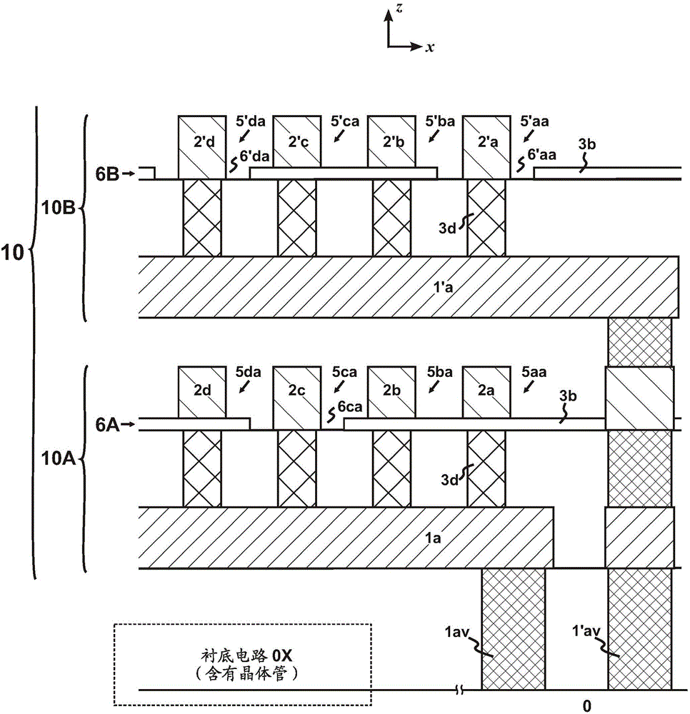
[0036] In order to reduce the number of data masks, the present invention proposes a three-dimensional offset printing memory (3D-oP). It uses offset printing method to enter data. The offset printing method is one of the printing methods. The main printing methods include photo-lithography and imprint-lithography (also known as nano-imprint lithogrpahy, referred to as NIL) (see Chinese patent application "Three-dimensional printing memory"): photolithography The method uses a data mask to input data; while imprinting records uses a data template (template, also known as master, stamp, or mold, etc.) to input data.

[0037] Figure 5A-Figure 5B Represents two printing steps used in an offset printing method. It uses a multi-region data mask8. In this embodiment, the multi-region data mask 8 contains mask patterns for two different storage layers 16A, 16B. They are respectively located in the data mask areas 8a, 8b.

[0038] The offset printing method includes the followi...


PUM


Abstract

The invention provides a three-dimensional offset-printed memory (3D-oP). Compared with a routine three-dimensional mask programmable read-only memory (3D-MPROM), the three-dimensional offset-printed memory is advantageous in that a relatively small amount of required data masks is realized, and a relatively low cost of the masks is required. Mask patterns which correspond with different storage layers / digital bits are combined in a multi-area data mask. In different printing steps, the offsets of a wafer relative to the multi-area data mask are different. Therefore, data patterns from one data mask are printed into data recording films of different storage layers / digital bits.

Description

technical field [0001] This invention relates to the field of integrated circuit memories and, more particularly, to mask-programmed read-only memories (mask-ROMs). Background technique [0002] Three-dimensional mask-programmed read-only memory (3D-MPROM) is an ideal medium for mass publishing. US Patent 5,835,396 discloses a 3D-MPROM. Such as figure 1 As shown, 3D-MPROM is a monolithic integrated circuit, which includes a semiconductor substrate 0 and a three-dimensional stack 10 stacked on the substrate. The three-dimensional stack 10 contains M (M≥2) storage layers (such as 10A, 10B) stacked on each other. Each storage layer (such as 10A) contains multiple top address lines (such as 2a), bottom address lines (such as 1a) and storage elements (such as 5aa). Each storage element stores n (n≥1) bits of data. The storage layer (such as 16A, 16B) is coupled with the substrate 0 through contact via holes (such as 1av, 1'av). The substrate circuit 0X in the substrate 0 co...

Claims


Application Information

Patent Timeline
Patent Type & Authority Applications(China)
IPC IPC(8): H01L27/112H01L21/8246
Inventor 张国飙
Owner HANGZHOU HAICUN INFORMATION TECH
Why Eureka
Try Eureka