


Quick Research
Generate reliable direction feasibility study reports for your R&D in just a few steps.

Technical Q&A
Discover and master advanced knowledge NOW. Basics, ideas, possibilities, all at once.

Find Solutions
As an expert in R&D theories, this can generate solutions to your technical problems instantly.

Evaluate Feasibility
Analyze your overall solution with one click, know your potential R&D risks in advance.

Monitor Landscape
Get weekly tech updates, stay abreast of the latest tech innovations and key insights.
Flip-chip led chip and preparation method thereof
A LED chip flip-chip technology, which is applied to electrical components, circuits, semiconductor devices, etc., can solve the problems of increasing light attenuation, reducing chip life, and difficult heat dissipation, etc., and achieves large flip-chip contact area, fast heat dissipation, and heat dissipation good effect
- Summary
- Abstract
- Description
- Claims
- Application Information
AI Technical Summary
Problems solved by technology
Method used
Image

Examples
Embodiment 1
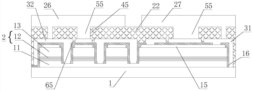
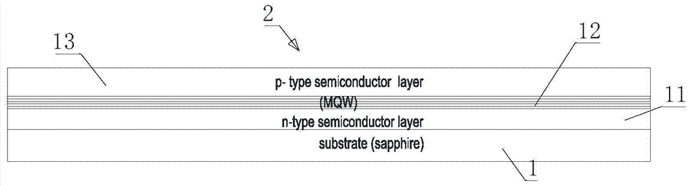
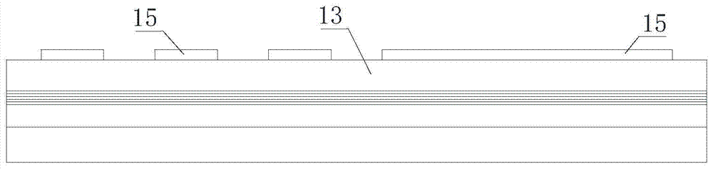
[0048] Such as figure 1 As shown, the flip-chip LED chip of this embodiment includes a substrate 1 and an N-type gallium nitride layer 11, a light-emitting layer 12, and a P-type gallium nitride layer 13 grown sequentially on the surface of the substrate 1, and the P-type gallium nitride layer The layer 13 covers the reflective layer 15 , and the N-type GaN layer 11 , the light-emitting layer 12 and the P-type GaN layer 13 constitute the epitaxial layer 2 . The first insulating layer 16 covers the surface of the epitaxial layer 2 and the reflective layer 15 . A P-type electrode 31 electrically connected to the reflective layer 15 and an N-type electrode 32 electrically connected to the N-type GaN layer 11 are formed on the first insulating layer 16 . An annular cooling groove 65 penetrating to the surface of the first insulating layer 16 is formed on the P-type electrode 31 or the N-type electrode 32 . The surface of the P-type electrode 31 and the N-type electrode 32 and th...
Embodiment 2
[0065] Such as Figure 10 As shown, the flip-chip LED chip of this embodiment includes a substrate 1 and an N-type gallium nitride layer 11, a light-emitting layer 12, and a P-type gallium nitride layer 13 grown sequentially on the surface of the substrate 1, and the P-type gallium nitride layer The layer 13 covers the current spreading layer 15 ′, and the N-type GaN layer 11 , the light-emitting layer 12 and the P-type GaN layer 13 form an epitaxial layer. The first insulating layer 16' is covered on the surface of the epitaxial layer and the current spreading layer 15'. A P-type electrode 31 electrically connected to the current spreading layer 15' and an N-type electrode 32 electrically connected to the N-type gallium nitride layer 11 are formed on the first insulating layer 16'. On the N-type electrode 32, an annular cooling groove 65 penetrating to the surface of the first insulating layer 16' is formed. The surface of the P-type electrode 31 and the N-type electrode 32...
Embodiment 3
[0068] Such as Figure 11a with Figure 11b As shown, the first five steps of the preparation steps of this embodiment are the same as those of Embodiment 1, and the difference from Embodiment 1 is that the heat dissipation groove 65 is located in the middle of the chip, while the heat dissipation grooves in Embodiment 1 are located at both ends of the chip. The heat dissipation groove 65 is formed on the N-type electrode 32 . Such as Figure 12 As shown, the second insulating layer 22 covers the P-type electrode 31 , the N-type electrode 32 and the surface of the first insulating layer 16 between the P-type electrode and the N-type electrode, and fills the heat dissipation groove 65 .
[0069] Such as Figure 13a with Figure 13b As shown, a P-type electrode contact hole 29 and an N-type electrode contact hole 28 are formed on the second insulating layer 22, as well as a heat dissipation hole 45 penetrating to the surface of the N-type electrode 32. The projection of the ...
PUM
 Abstract
Description
Claims
Application Information
 - R&D Engineer
- R&D Manager
- IP Professional
- Industry Leading Data Capabilities
- Powerful AI technology
- Patent DNA Extraction
Browse by: Latest US Patents, China's latest patents, Technical Efficacy Thesaurus, Application Domain, Technology Topic, Popular Technical Reports.
© 2024 PatSnap. All rights reserved.Legal|Privacy policy|Modern Slavery Act Transparency Statement|Sitemap|About US| Contact US: help@patsnap.com