Flip-chip high-voltage LED chip and preparation method thereof

A technology of LED chips and chips, applied in electrical components, circuits, semiconductor devices, etc., can solve the problems of heat conduction and reliability of LED high-voltage chips that have not been solved, affect chip reliability, and difficult to export heat, and achieve good heat dissipation effect. , Guaranteed reliability, fast heat dissipation effect

Active Publication Date: 2017-08-25
ELEC TECH PHOTOELECTRIC TECH DALIAN
View PDF1 Cites 0 Cited by
  • Summary
  • Abstract
  • Description
  • Claims
  • Application Information

AI Technical Summary

Problems solved by technology

The above-mentioned LED flip-chip high-voltage chip mainly dissipates heat through conduction, but its second insulating layer is made of organic silica gel with a thickness greater than 6um. Because the second insulating layer is thick and has a low thermal conductivity, it is still difficult to dissipate the heat, and the heat gathers in the chip. It will affect the reliability of the chip, increase the light decay and reduce the life of the chip, and the heat conduction and reliability problems of the LED high-voltage chip have not been resolved.

Method used


Image

  • Flip-chip high-voltage LED chip and preparation method thereof
  • Flip-chip high-voltage LED chip and preparation method thereof
  • Flip-chip high-voltage LED chip and preparation method thereof

Examples


Embodiment Construction

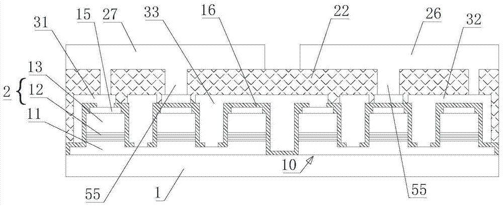
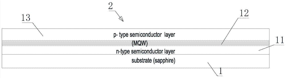
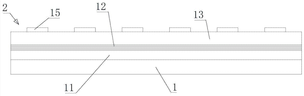
[0040] Such as figure 1 As shown, the flip-chip high-voltage LED chip of the present invention includes a substrate 1 and M chips 10 located on the surface of the substrate 1 that are insulated and independent from each other, M is an integer greater than or equal to 2, and each chip 10 includes 1 N-type gallium nitride layer 11, light-emitting layer 12 and P-type gallium nitride layer 13 on the surface, P-type gallium nitride layer 13 covered with reflective layer 15, N-type gallium nitride layer 11, light-emitting layer 12 and P-type gallium nitride layer 13 The GaN-type GaN layer 13 constitutes the epitaxial layer 2 of each chip. Each chip is separated by a trench 3 whose depth reaches the surface of the substrate 1 . The surface of the epitaxial layer 2 and the reflective layer 15 of each chip is covered with the first insulating layer 16 . On the first insulating layer 16, form the P lead electrode 31 electrically connected with the reflection layer 15 of the first chip...


PUM


Abstract

The invention discloses an inverted high-voltage LED chip and a preparation method thereof. The inverted high-voltage LED chip comprises a substrate and M chips, wherein each chip comprises an N-type gallium nitride layer, a luminous layer, a P-type gallium nitride layer, a reflecting layer, a first insulating layer, a P lead electrode, an N lead electrode and a P-N lead connecting electrode; heat radiation grooves are formed in the P lead electrodes and / or the N lead electrodes and / or the P-N lead connecting electrodes; the second insulating layers cover the surfaces of the P lead electrodes, the P-N lead connecting electrodes and the N lead electrodes and the surfaces of the first insulating layers among the P lead electrodes, the P-N lead connecting electrodes and the N lead electrodes, and fill the heat radiation grooves; heat radiation holes are formed in the second insulating layers; the projection of the heat radiation holes on the horizontal plane is positioned inside the heat radiation grooves; the second insulating layers are deposited on N bonding pads and P bonding pads; the heat radiation holes are filled with heat conduction columns; the heat conduction columns are connected with the P bonding pads and the N bonding pads. Due to the adoption of the heat radiation columns among the P bonding pads, the N bonding pads and the lead electrodes, the inverted high-voltage LED chip is relatively high in heat radiation speed and small in heat radiation amount.

Description

technical field [0001] The invention belongs to the technical field of semiconductor optoelectronic chips, and in particular relates to a flip-chip high-voltage LED chip and a preparation method thereof. Background technique [0002] With the continuous improvement of LED (Light Emitting Diode) luminous efficiency, LED has become one of the most valued light sources in recent years. With the development of LED technology, LEDs directly driven by high voltage have been realized. The efficiency of high-voltage LEDs is better than that of traditional low-voltage LEDs, mainly due to the small current and multi-unit design that can spread the current evenly, and high-voltage LEDs can realize direct high-voltage drive, thereby saving the cost of LED drive. [0003] Existing high-voltage LED chips have the problems of increased power, difficult heat dissipation, and reduced reliability. To address these problems, the industry has made further improvements to the structure of high-...

Claims


Application Information

Patent Timeline
Patent Type & Authority Patents(China)
IPC IPC(8): H01L33/64H01L33/36
CPCH01L33/36H01L33/64H01L33/642
Inventor 王冬雷陈顺利莫庆伟
Owner ELEC TECH PHOTOELECTRIC TECH DALIAN
Why Eureka
Try Eureka