Preparation method of intermetallic compound thin film
A technology of intermetallic compounds and thin films, which is applied in the field of preparation of intermetallic compound thin films, can solve the problems of slow growth rate, high energy consumption and high cost of thin films, and achieve the effects of accelerated growth rate, fast growth rate and improved mechanical properties
- Summary
- Abstract
- Description
- Claims
- Application Information
AI Technical Summary
Problems solved by technology
Method used
Image
Examples
Embodiment 1
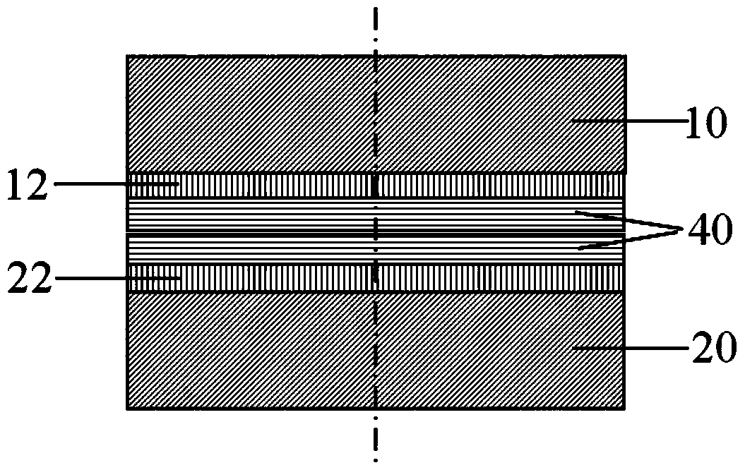
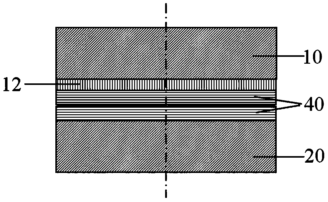
[0044] Such as figure 1 and image 3Shown, the preparation method of intermetallic compound thin film of the present invention can be realized by following specific processing steps:
[0045] Step 1: Provide a polycrystalline Cu first metal substrate, sputter a 0.25 μm thick Sn first solder metal layer on the polycrystalline Cu first metal substrate; provide a polycrystalline Cu second metal substrate, and sputter on the polycrystalline Cu first metal substrate. Sputtering a 0.25 μm thick Sn second solder metal layer on the crystal Cu second metal substrate;
[0046] Step 2: coating flux on the surfaces of the first Sn solder metal layer and the Sn second solder metal layer;
[0047] Step 3: Aligning the first Sn solder metal layer and the Sn second solder metal layer, and placing them in contact to form an assembly;
[0048] Step 4: Heat the assembly formed in Step 3 to 250° C. for brazing reflow, and make the temperature of the polycrystalline Cu first metal substrate low...
Embodiment 2
[0052] Such as figure 1 and image 3 Shown, the preparation method of intermetallic compound thin film of the present invention can be realized by following specific processing steps:
[0053] Step 1: providing a polycrystalline Cu first metal substrate, electroplating a 10 μm thick Sn-Cu first solder metal layer on the polycrystalline Cu first metal substrate; providing a polycrystalline Cu second metal substrate, on the polycrystalline Cu first metal substrate, Electroplating a 10 μm thick Sn-Cu second solder metal layer on the Cu second metal substrate;
[0054] Step 2: Coating flux on the surfaces of the first Sn-Cu solder metal layer and the Sn-Cu second solder metal layer;
[0055] Step 3: aligning the Sn-Cu first solder metal layer and the Sn-Cu second solder metal layer, and placing them in contact to form an assembly;
[0056] Step 4: Heat the assembly formed in Step 3 to 250° C. for brazing reflow, and make the temperature of the polycrystalline Cu first metal sub...
Embodiment 3
[0060] Such as figure 1 and image 3 Shown, the preparation method of intermetallic compound thin film of the present invention can be realized by following specific processing steps:
[0061] Step 1: Provide a polycrystalline Cu first metal substrate, electroplate a 30 μm thick Sn first solder metal layer on the polycrystalline Cu first metal substrate; provide a polycrystalline Cu second metal substrate, and Electroplating a second solder metal layer of Sn with a thickness of 30 μm on the second metal base;
[0062] Step 2: coating flux on the surfaces of the first Sn solder metal layer and the Sn second solder metal layer;
[0063] Step 3: Aligning the first Sn solder metal layer and the Sn second solder metal layer, and placing them in contact to form an assembly;
[0064] Step 4: Heat the assembly formed in Step 3 to 250° C. for brazing reflow, and make the temperature of the polycrystalline Cu first metal substrate lower than the temperature of the polycrystalline Cu ...
PUM
| Property | Measurement | Unit |
|---|---|---|
| thickness | aaaaa | aaaaa |
Abstract
Description
Claims
Application Information
 - Generate Ideas
- Intellectual Property
- Life Sciences
- Materials
- Tech Scout
- Unparalleled Data Quality
- Higher Quality Content
- 60% Fewer Hallucinations
Browse by: Latest US Patents, China's latest patents, Technical Efficacy Thesaurus, Application Domain, Technology Topic, Popular Technical Reports.
© 2025 PatSnap. All rights reserved.Legal|Privacy policy|Modern Slavery Act Transparency Statement|Sitemap|About US| Contact US: help@patsnap.com


