A Pulse Width Adaptive Configurable Memory IP Structure

A self-adaptive, memory technology, applied in static memory, digital memory information, information storage, etc., can solve the problems of unoptimized IP working pulse width, device performance impact, etc., to achieve fast read time, optimized device performance, low read The effect of power consumption

Active Publication Date: 2017-09-05
BEIJING MXTRONICS CORP +1
View PDF5 Cites 0 Cited by
  • Summary
  • Abstract
  • Description
  • Claims
  • Application Information

AI Technical Summary

Problems solved by technology

In different environments, the memory IP structure is affected by the environment, and the pulse width required for normal read / write operations is different, and the fixed pulse is generated in the design stage. In order to ensure the reliability of the device, a large design margin is reserved. Therefore, The pulse width of the IP working in different environments is not optimized, which has a certain impact on the performance of the device

Method used


Image

  • A Pulse Width Adaptive Configurable Memory IP Structure
  • A Pulse Width Adaptive Configurable Memory IP Structure
  • A Pulse Width Adaptive Configurable Memory IP Structure

Examples


Embodiment Construction

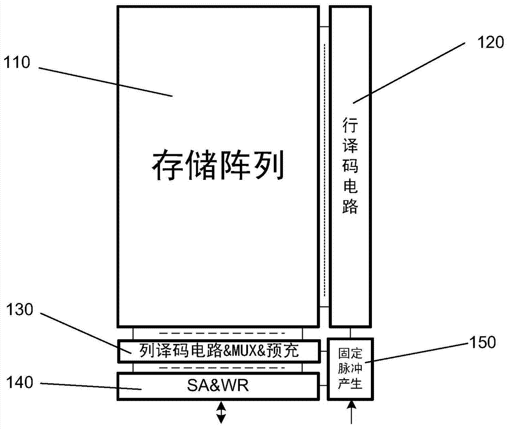
[0028] like figure 1 As shown, the traditional memory IP circuit structure includes a memory array 110 , a row decoding circuit 120 , a column decoding & MUX & precharging circuit 130 , a sensitive amplifier SA & WR 140 and a fixed pulse generator 150 . Fixed pulse generation 150 generates control pulses with fixed pulse width T during IP read / write operations, and sends them to row decoding circuit 120, column decoding & MUX & pre-charging circuit 130, sensitive amplifier SA & WR 140 to generate pulsed IP reading and writing timing. During the IP read operation, the row decoding circuit 120 generates a unique row strobe signal, which is used to strobe the only memory cell row in the memory array, and the selected row unit is turned on and discharges the connected bit line pair , and generate the bit line pair voltage difference; the column decoding & MUX & precharge circuit 130 generates a unique column strobe signal for each group of MUX, which is used to transmit the bit l...


PUM


Abstract

A pulse width self-adaptive configurable memory IP structure, including a memory array (10), a sensitive amplification and read / write circuit SA&WR (11), a row decoding circuit (12), a column decoding & MUX & precharging circuit (14), Optimized configuration circuit (20), pulse configuration module (22), drive (24), 1 dummy cell row (25), n dummy cell columns (26), sensitive amplifier SA with preset function (27). When the pulse width self-adaptive configurable memory IP structure of the present invention is powered on, an internal read operation with different pulse widths is generated through the optimized configuration circuit (20) built in the memory IP structure, and the read-back data is looked up and analyzed to finally determine The optimized pulse width of the memory IP structure suitable for the working environment of the device, the invention optimizes the memory reading timing at a certain chip area cost, and further optimizes the reading speed and dynamic power consumption of the memory IP structure.

Description

technical field [0001] The invention relates to a memory IP structure, in particular to a configurable memory IP structure with self-adaptive pulse width. Background technique [0002] The traditional memory IP structure mainly includes storage array, row decoding circuit, column decoding & MUX & pre-charging circuit, sensitive amplifier SA & WR and fixed pulse generation. The pulse mode is used to control the working sequence of the device. The fixed pulse is generated during the IP read / write operation , Generate a control pulse with a fixed pulse width T, and send it to the row decoding circuit, column decoding & MUX & pre-charging circuit, sensitive amplifier SA & WR respectively, and generate the read and write timing of pulsed IP. During the read operation of the IP, the row decoding circuit generates a unique row strobe pulse signal for the gating of the memory cell row. The selected row unit is turned on and discharges the connected bit line pair, and generates a bit...

Claims


Application Information

Patent Timeline
Patent Type & Authority Patents(China)
IPC IPC(8): G11C7/22
Inventor 谭建平赵元富陆时进李建成李阳李鹏李晓磊刘琳张晓晨
Owner BEIJING MXTRONICS CORP
Why Eureka
Try Eureka