Charge protection circuit for capacitor step-down
A charging protection and capacitor step-down technology, which is applied to battery circuit devices, circuit devices, collectors, etc., can solve the problems of battery damage, easy overcharging, and no cost advantage, so as to prolong service life, improve product performance, reduce The effect of material cost
- Summary
- Abstract
- Description
- Claims
- Application Information
AI Technical Summary
Problems solved by technology
Method used
Image
Examples
Embodiment 1
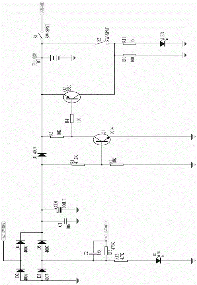
[0036] Such as figure 1As shown, the reverse switching element is a 4007 type rectifier diode D1; the battery overcharge detection circuit is composed of a 9014NPN type first transistor Q1, a first resistor R1, and a second resistor R2, and the battery over-full current The circuit is composed of an 8550PNP second transistor Q2, a third resistor R3 and a fourth resistor R4, wherein the first resistor R1 and the second resistor R2 are connected in series to form a voltage divider circuit between the output terminal of the rectifier circuit and the ground terminal Between, the base of the first transistor Q1 is connected to the connection point of the first resistor R1 and the second resistor R2, its emitter is grounded, one of its collectors is connected to the output terminal of the rectifier circuit through the third resistor R3, and the other is connected to the output terminal of the rectifier circuit through the fourth resistor R4 is connected to the base of the second tra...
Embodiment 2
[0040] Such as figure 2 As shown, this embodiment is the same as the embodiment 1 except that the setting position of the rectifier diode D1 is different from that of the embodiment 1, which is a modification of the embodiment 1. Wherein, the positive terminal of the rectifying diode D1 is connected to the output terminal of the rectifying circuit, and the negative terminal thereof is connected to the emitter of the second transistor Q2.
Embodiment 3
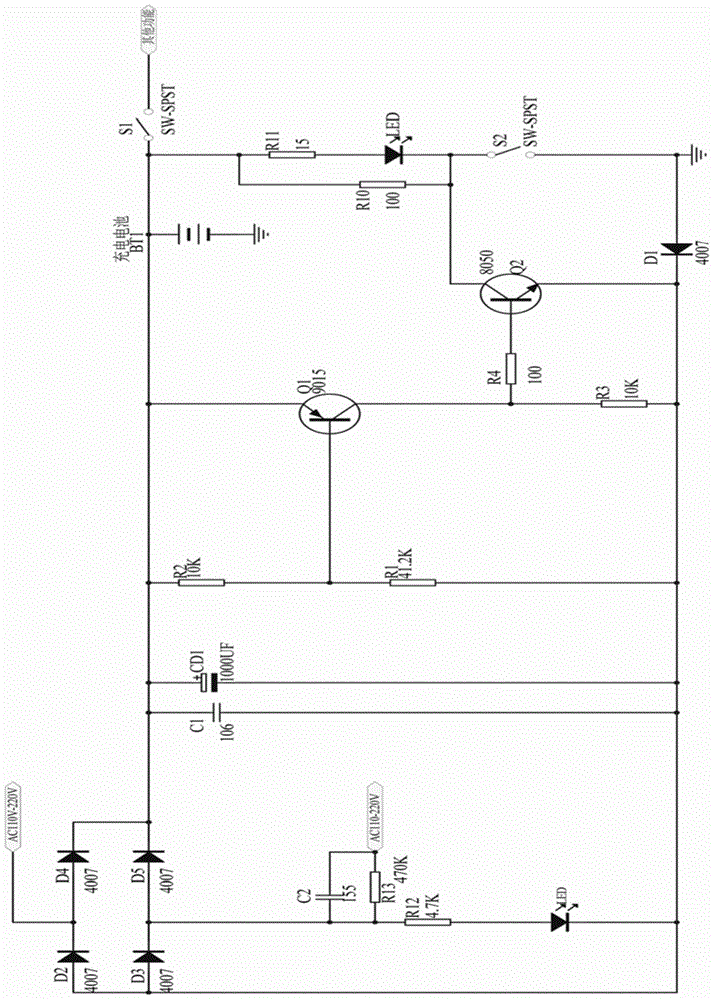
[0042] Such as image 3 As shown, this embodiment is the same as that of embodiment 1 except that the setting position of rectifier diode D1 and the models of first transistor Q1 and second transistor Q2 are different from embodiment 1, which is a modification of embodiment 1. Program. Wherein, the models of the first transistor Q1 and the second transistor Q2 are respectively a 9015 model PNP transistor and an 8050 model NPN transistor.
[0043] The positive terminal of the rectifier diode D1 in this embodiment is grounded; the first resistor R1 and the second resistor R2 are connected in series to form a voltage divider circuit between the output terminal of the rectifier circuit and the negative terminal of the rectifier diode D1, and the first transistor Q1 The base is connected to the connection point of the first resistor R1 and the second resistor R2, the emitter is connected to the output terminal of the rectifier circuit, one of the collectors is connected to the neg...
PUM
 Abstract
Description
Claims
Application Information
 - R&D
- Intellectual Property
- Life Sciences
- Materials
- Tech Scout
- Unparalleled Data Quality
- Higher Quality Content
- 60% Fewer Hallucinations
Browse by: Latest US Patents, China's latest patents, Technical Efficacy Thesaurus, Application Domain, Technology Topic, Popular Technical Reports.
© 2025 PatSnap. All rights reserved.Legal|Privacy policy|Modern Slavery Act Transparency Statement|Sitemap|About US| Contact US: help@patsnap.com


