
Spot size converter and optical apparatus

A technology of optical devices and converters, applied in optics, optical components, instruments, etc., can solve problems such as high coupling loss and achieve low-loss coupling effects

Inactive Publication Date: 2015-04-29
FUJITSU LTD
View PDF11 Cites 10 Cited by
  • Summary
  • Abstract
  • Description
  • Claims
  • Application Information

AI Technical Summary

Problems solved by technology

Therefore, an excessively high coupling loss occurs

Method used


Image

  • Spot size converter and optical apparatus
  • Spot size converter and optical apparatus
  • Spot size converter and optical apparatus

Examples


Embodiment Construction

[0032] Hereinafter, a spot size converter and an optical device according to an embodiment of the present invention are described with reference to the accompanying drawings.

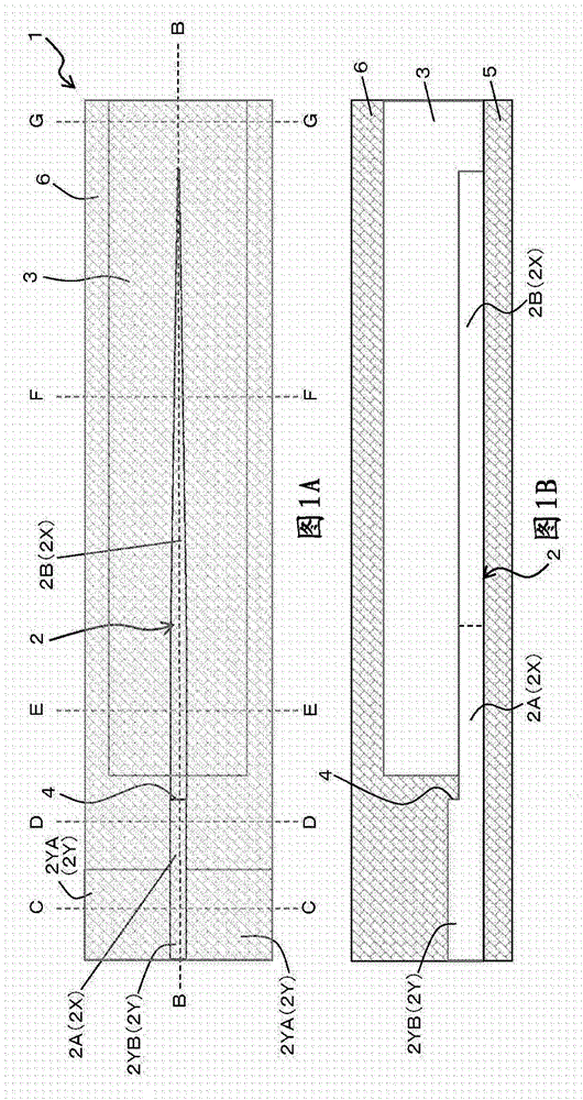
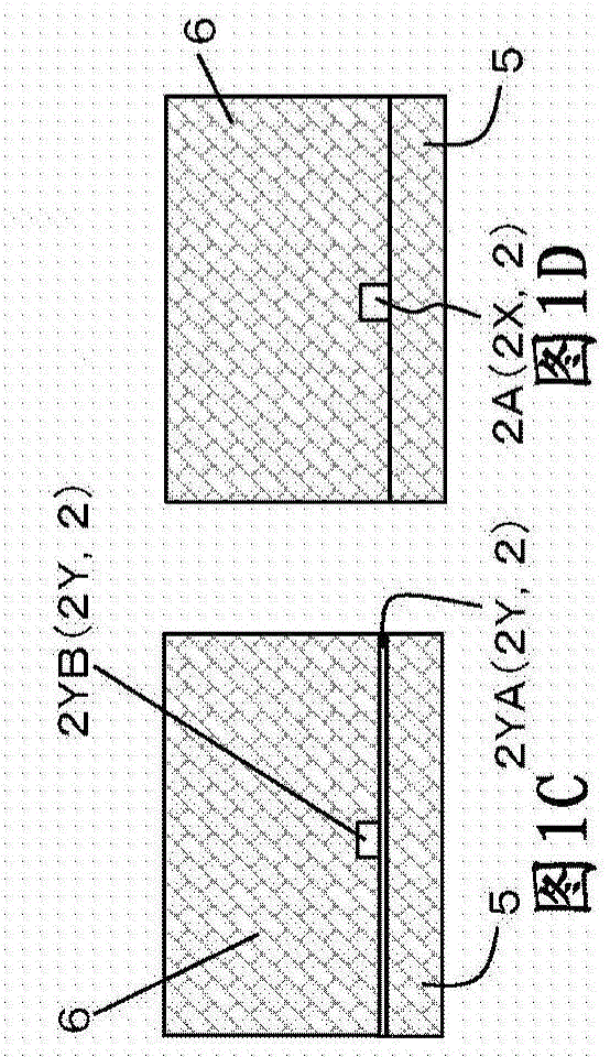
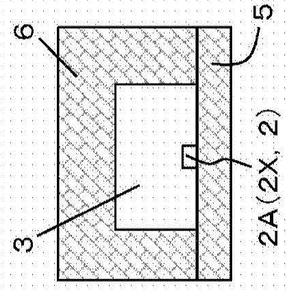
[0033] First, refer to Figure 1A to Figure 22 The spot size converter according to the present embodiment is described.

[0034] The spot size converter according to the present embodiment is a second core type spot size converter in which the width of the silicon waveguide core is reduced in a tapered shape, and the silicon waveguide core is covered with a second core so that light travels from the silicon waveguide core to the second core. Rollover to enlarge the spot size. In such a second core type spot size converter as just described, light gradually transits from the silicon waveguide core to the second core in the region where the width of the silicon waveguide core decreases in a tapered shape, eventually the light completely Go beyond the second core to enlarge the spot size. For example, ...


PUM


Abstract

A spot size converter includes a first silicon waveguide core that includes a width-fixed region having a fixed width and a width-tapered region continuing to the width-fixed region and having a width reducing toward a terminal portion, and a second waveguide core continuing to the first silicon waveguide core and covering at least the width-tapered region. The first silicon waveguide core has a thickness-wise step in the width-fixed region.

Description

technical field [0001] Embodiments discussed herein relate to a spot size converter and optical device. Background technique [0002] In recent years, due to the promotion of high-definition video distribution and the like, the amount of information has been and is rapidly increasing, and this requires improvement in information processing performance of data centers and the like. In addition, this requires low-cost and low-power devices to achieve an increase in information processing performance, and, in recent years, silicon photonics has been actively researched. [0003] Because the cross-sectional shape of a silicon waveguide core for silicon photonics like the one just described is so small, eg, about 500 nm in width and about 220 nm in height, a mismatch with the spot size of the fiber (eg, about a few μm to 10 μm) occurs. Therefore, an excessively high coupling loss occurs. [0004] Therefore, in order to suppress excessively high coupling loss, a spot size conver...

Claims


Application Information

Patent Timeline
IPC IPC(8): G02B6/42
CPCG02B6/305G02B2006/12061G02B6/12016
Inventor 松本武关口茂昭
Owner FUJITSU LTD
Learn More