A kind of nitride LED epitaxial wafer structure and its preparation method based on copper substrate
A technology of LED epitaxial wafer and nitride epitaxial layer, which is applied in the direction of electrical components, circuits, semiconductor devices, etc., can solve the problems of expensive equipment, complicated process, and low process yield, and achieve the effect of cost saving
- Summary
- Abstract
- Description
- Claims
- Application Information
AI Technical Summary
Problems solved by technology
Method used
Image
Examples
preparation example Construction
[0068] A method for preparing a nitride LED epitaxial wafer structure based on a copper substrate, comprising the following steps:
[0069] 1) Prepare one or more two-dimensional derived film layers on a copper substrate to obtain a copper substrate with a two-dimensional derived film layer; specifically include three preparation methods:
[0070] Preparation method 1, directly using chemical vapor deposition on the copper substrate to prepare one or more graphene layers or hexagonal boron nitride layers;
[0071] The specific steps for preparing the graphene layer are as follows: the copper substrate is placed in a chemical vapor deposition system, and at a temperature of 400-1050 ° C, argon and hydrocarbons are simultaneously introduced to form a graphene layer on the copper substrate. graphene layer;
[0072] The specific steps for preparing hexagonal boron nitride are as follows: put the copper substrate into a chemical vapor deposition system, and at a temperature of 400...
Embodiment 1
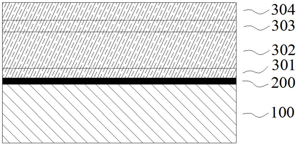
[0088] like figure 1 As shown, on top of a 2-inch, 80 μm thick copper substrate wafer 100, a single layer of graphene 201 is used as a two-dimensional derived film, and on the two-dimensional derived film is a nitride blue LED epitaxial layer. Wherein, the buffer layer 301 is made of 200nm n-type Al 0.1 Ga 0.9 N-layer composition; the structural parameters of the n-type electron injection layer 302 are as follows: a 2 μm thick n-type GaN layer, the doping element is Si, and the doping concentration is 1.0×10 19 ; The structural parameters of the active layer 303 are as follows: In 0.15 Ga 0.85 N / GaN multiple quantum well light-emitting layer, In 0.15 Ga 0.85 The single-layer thicknesses of N and GaN are 3nm and 10nm respectively, and the number of periods of the multiple quantum wells is 5; the structural parameters of the p-type hole injection layer 304 are as follows: it includes two sublayers, one is a 0.2 μm thick p-type GaN layer, The p-type doping element is Mg, an...
Embodiment 2
[0093] like image 3 As shown, on top of a 4-inch, 200 μm thick copper substrate wafer 100, a multi-layer hexagonal boron nitride (h-BN) 202 is used as a two-dimensional derived film, and a nitride blue LED is placed on the two-dimensional derived film epitaxial layer. Among them, the buffer layer 301 is made of 150nm n-type Al 0.3 Ga 0.7 N-layer structure; the structural parameters of the n-type electron injection layer 302 are as follows: a 2.5 μm thick n-type GaN layer, the doping element is Si, and the doping concentration is 1.5×10 19 ; The structural parameters of the active layer 303 are as follows: In 0.15 Ga 0.85 N / GaN multiple quantum well light-emitting layer, In 0.15 Ga 0.85 The single-layer thicknesses of N and GaN are 3nm and 10nm respectively, and the number of periods of the multiple quantum wells is 5; the structural parameters of the p-type hole injection layer 304 are as follows: it includes two sublayers, one is a 0.2 μm thick p-type GaN layer, The p...
PUM
| Property | Measurement | Unit |
|---|---|---|
| thickness | aaaaa | aaaaa |
| thickness | aaaaa | aaaaa |
| thickness | aaaaa | aaaaa |
Abstract
Description
Claims
Application Information
 - R&D
- Intellectual Property
- Life Sciences
- Materials
- Tech Scout
- Unparalleled Data Quality
- Higher Quality Content
- 60% Fewer Hallucinations
Browse by: Latest US Patents, China's latest patents, Technical Efficacy Thesaurus, Application Domain, Technology Topic, Popular Technical Reports.
© 2025 PatSnap. All rights reserved.Legal|Privacy policy|Modern Slavery Act Transparency Statement|Sitemap|About US| Contact US: help@patsnap.com


