Preparation method of thin film transistor of liquid crystal display panel and liquid crystal display panel

A technology for liquid crystal display panels and thin film transistors, which is applied in semiconductor/solid-state device manufacturing, semiconductor devices, optics, etc., can solve problems such as electrostatic breakdown and burning of TFT film layers, and achieve the effect of not easy electrostatic breakdown.

Active Publication Date: 2017-05-31
HEFEI XINSHENG OPTOELECTRONICS TECH CO LTD +1
View PDF3 Cites 0 Cited by
  • Summary
  • Abstract
  • Description
  • Claims
  • Application Information

AI Technical Summary

Problems solved by technology

[0002] For example, in the process of oxide TFT (Oxide TFT), because the static charge accumulated in the metal island (the voltage input point of the storage capacitor electrode of each pixel) on the ITO layer of the thin film transistor cannot be released, it is easy to cause severe Electrostatic breakdown (ESD), which burns the nearby TFT film layer

Method used


Image

  • Preparation method of thin film transistor of liquid crystal display panel and liquid crystal display panel
  • Preparation method of thin film transistor of liquid crystal display panel and liquid crystal display panel
  • Preparation method of thin film transistor of liquid crystal display panel and liquid crystal display panel

Examples


no. 1 example

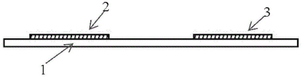
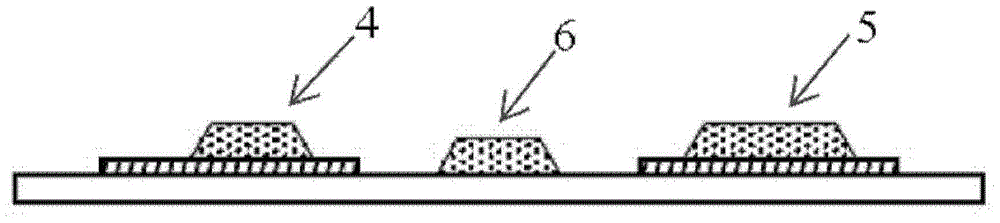
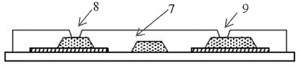
[0063] Referring to FIG. 2 , it shows a schematic diagram of a method for manufacturing a thin film transistor for a liquid crystal display panel according to a first embodiment of the present invention. Figure 2a-2e A schematic cross-sectional view of a thin film transistor obtained through multiple steps in the first embodiment is shown. Here, as mentioned above, the connection of the base electrodes of two adjacent pixels is also used as an example for the corresponding description, and only the corresponding structural arrangement is shown in the accompanying drawings.

[0064] see Figure 2a , a first ITO layer having a predetermined pattern is formed on the substrate 21 for a liquid crystal display panel in the same manner as in the prior art. As shown in the figure, two spaced-apart regions 22 , 23 of the first ITO layer are formed on the illustrated substrate 21 . It should be noted that a plurality of spaced-apart regions can be formed on the substrate 21 to form a ...

no. 2 example

[0072] Referring to FIG. 3 , it shows a schematic diagram of a method for manufacturing a thin film transistor for a liquid crystal display panel according to a second embodiment of the present invention. Figures 3a-3g A schematic cross-sectional view of a thin film transistor obtained through multiple steps in the second embodiment is shown.

[0073] see Figure 3a , a first ITO layer having a predetermined pattern is formed on the substrate 41 of the liquid crystal display panel in the same manner as in the prior art. As shown, two spaced-apart regions 42 , 43 of the first ITO layer are formed on the illustrated substrate 41 . It should be noted that a plurality of spaced-apart regions may be formed on the substrate 41 , and here only two spaced-apart regions are shown for the purpose of illustration and description. A gate metal layer is deposited, and the mask of the gate is changed to increase the connection line portion between the metal island and the gate wire. In ...


PUM


Abstract

The invention discloses a preparation method of a thin film transistor of a liquid crystal display panel. The method comprises the step that a first ITO layer, a grid layer, a grid insulation layer, an active layer, an etch stopper layer, a source and drain layer, a passivation layer and a second ITO layer are sequentially prepared on a substrate of the liquid crystal display panel. In the preparation step of the grid layer, a metal island and a base wire which are located on two spaced areas of the first ITO layer and a grid wire located at the position, between two spaced areas, of the substrate are formed, and at the same time, the grid wire and the metal island are connected through a connection line. Under the situation that a contact hole of the connection line and contact holes of the base wire and the metal island are located in the same section, the metal island and the base wire are connected through the second ITO layer. In addition, the invention provides the liquid crystal display panel prepared according to the method.

Description

technical field [0001] The invention relates to the field of liquid crystal display, in particular to a preparation method of a thin film transistor used in a liquid crystal display panel and a corresponding liquid crystal display panel. Background technique [0002] For example, in the process of oxide TFT (Oxide TFT), because the static charge accumulated in the metal island (the voltage input point of the storage capacitor electrode of each pixel) on the ITO layer of the thin film transistor cannot be released, it is easy to cause severe Electrostatic breakdown (ESD), thus burning the nearby TFT film layer. [0003] In view of this, there is a real need to provide a method for preparing a thin film transistor used in a liquid crystal display panel and a liquid crystal display panel prepared by the method, which can at least partially solve the above problems. Contents of the invention [0004] The purpose of the present invention is to solve at least one aspect of the ...

Claims


Application Information

Patent Timeline
Patent Type & Authority Patents(China)
IPC IPC(8): H01L21/336H01L21/34H01L21/28H01L21/44
CPCG02F1/13H01L21/28H01L21/768H01L29/66772
Inventor 徐大林郑载润李根范张福刚
Owner HEFEI XINSHENG OPTOELECTRONICS TECH CO LTD
Why Eureka
Try Eureka