Wire gating polaroid, manufacturing method of wire gating polaroid, display panel and display device
A technology of wire grid polarizer and display panel, which is applied in the direction of nonlinear optics, optics, polarizing elements, etc., can solve the problems of low light utilization rate of liquid crystal display devices, avoid light leakage around the periphery, improve light utilization rate, and be easy to implement Effect
- Summary
- Abstract
- Description
- Claims
- Application Information
AI Technical Summary
Problems solved by technology
Method used
Image
Examples
Embodiment 1
[0050] This embodiment provides a wire grid polarizer and a corresponding preparation method of the wire grid polarizer. The wire grid polarizer has a wire grid structure arranged at intervals, so it can form a partial light-transmitting area, thereby controlling light more flexibly of the shot.
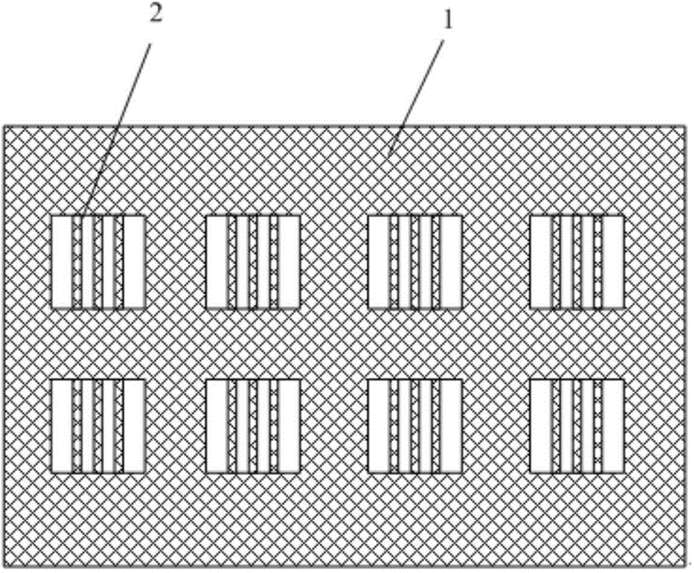
[0051] Such as figure 1 As shown, the wire grid polarizer includes a substrate 1, and the wire grid structure 2 arranged in an array is arranged at intervals in the substrate 1. The wire grid structure 2 allows light to pass through, and the substrate 1 except the wire grid structure 2 Other areas are continuous opaque structures.
[0052] Wherein, the thickness range of the substrate 1 is 20-250nm. Preferably, in the wire grid structure 2 , the width of the grid line is in the range of 25-250 nm, and the width of the grid pitch is in the range of 25-250 nm.
[0053]In order to ensure the strength of the wire grid polarizer and the light reflection and recycling in the opaque area...
Embodiment 2
[0071] This embodiment provides a display panel, which includes the wire grid polarizer in Embodiment 1. The display panel can effectively reduce the light absorption rate, and can also avoid light leakage around the non-sub-pixel area, and has better display effect.
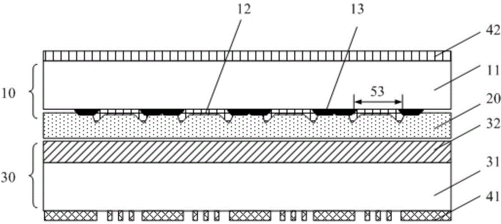
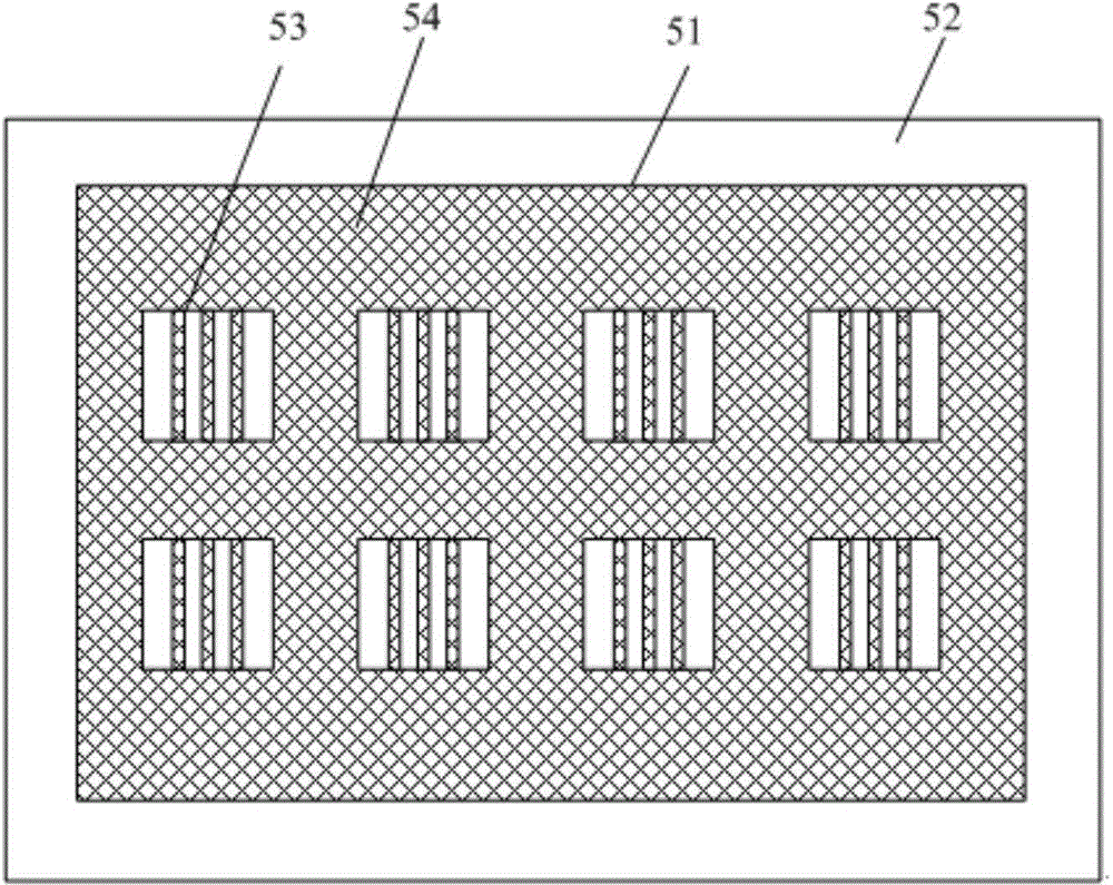
[0072] Such as image 3 As shown, the display panel includes a display area 51 (Active Area, referred to as AA area) and a non-display area 52 around the periphery of the display area, that is, the display area 51 is surrounded by the inside of the non-display area 52; figure 2 The area of the display panel corresponding to the display area 51 is provided with a polarizer 41 , and the polarizer 41 is a wire grid polarizer with a wire grid structure (WG for short) in Embodiment 1.
[0073] Wherein, the display area 51 includes a plurality of sub-pixel areas 53 arranged at intervals, the area of the polarizer 41 corresponding to the sub-pixel area 53 has a wire grid structure, and the other area is a metal t...
Embodiment 3
[0088] This embodiment provides a display panel. Compared with Embodiment 2, the disposition position of the polarizer in the display panel is different from the disposition position of the polarizer in the display panel of Embodiment 2. The display panel can effectively reduce light absorptivity, and can also avoid light leakage around the non-sub-pixel area, and has better display effect.
[0089] In the display panel of this embodiment, the polarizer is located relatively above the array substrate. Such as Figure 4 As shown, the polarizer 41 is disposed between the TFT array 32 and the second substrate 31 , and an insulating layer 33 is disposed between the polarizer 41 and the TFT array 32 . Form a layer of insulating layer 33 above the polarizer 41, and use the insulating layer 33 to separate the polarizer 41 from the thin film transistor array 32, so as to prevent the metal forming the polarizer 41 from affecting the control function of the thin film transistor array 3...
PUM
 Abstract
Description
Claims
Application Information
 - R&D
- Intellectual Property
- Life Sciences
- Materials
- Tech Scout
- Unparalleled Data Quality
- Higher Quality Content
- 60% Fewer Hallucinations
Browse by: Latest US Patents, China's latest patents, Technical Efficacy Thesaurus, Application Domain, Technology Topic, Popular Technical Reports.
© 2025 PatSnap. All rights reserved.Legal|Privacy policy|Modern Slavery Act Transparency Statement|Sitemap|About US| Contact US: help@patsnap.com


