


Quick Research
Generate reliable direction feasibility study reports for your R&D in just a few steps.

Technical Q&A
Discover and master advanced knowledge NOW. Basics, ideas, possibilities, all at once.

Find Solutions
As an expert in R&D theories, this can generate solutions to your technical problems instantly.

Evaluate Feasibility
Analyze your overall solution with one click, know your potential R&D risks in advance.

Monitor Landscape
Get weekly tech updates, stay abreast of the latest tech innovations and key insights.
Substrate etching method
A substrate and main etching technology, which is applied in the direction of electrical components, semiconductor/solid-state device manufacturing, circuits, etc., can solve the problems of shape defects, no cleaning effect, etc., and achieve the effect of reducing defects, reducing defects, and improving production capacity
- Summary
- Abstract
- Description
- Claims
- Application Information
AI Technical Summary
Problems solved by technology
Method used
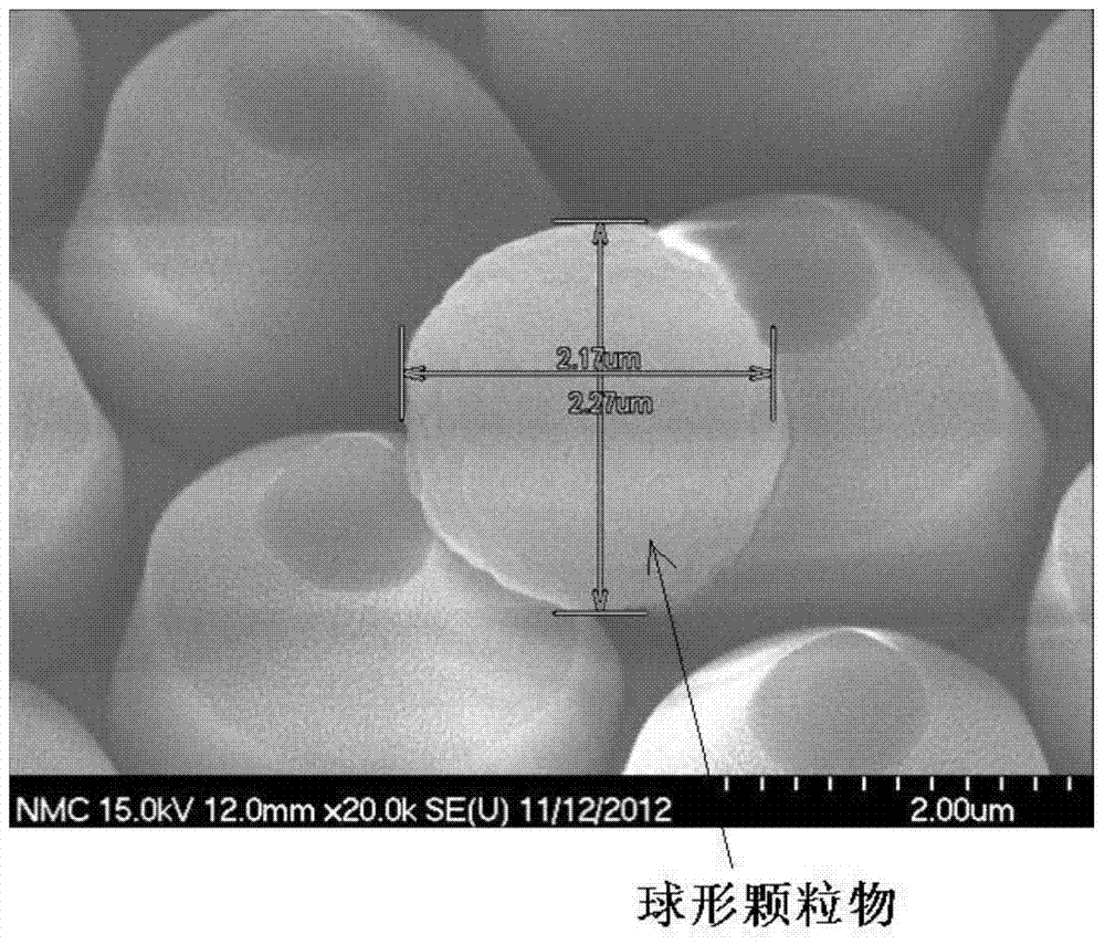
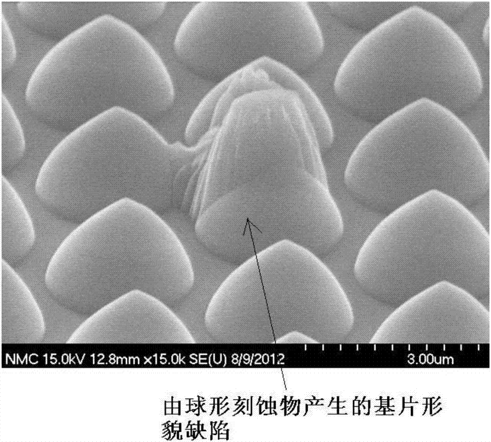
Image

Examples
Embodiment Construction
[0047] In order for those skilled in the art to better understand the technical solution of the present invention, the substrate etching method provided by the present invention will be described in detail below in conjunction with the accompanying drawings.
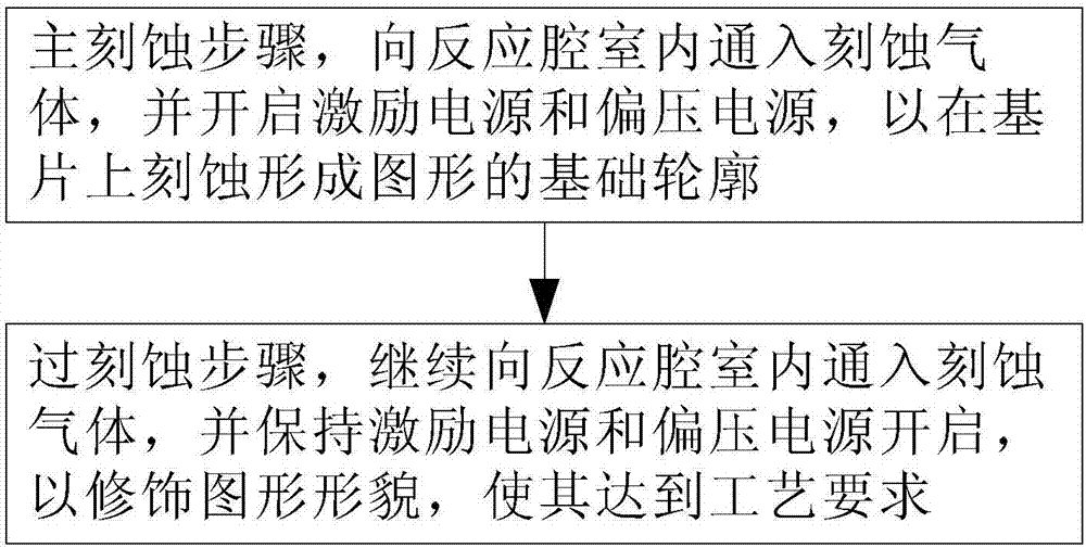
[0048] figure 2 A flowchart of a method for etching a substrate provided by an embodiment of the invention. see figure 2 , the substrate etching method comprises the following steps:
[0049] In the main etching step, the etching gas is introduced into the reaction chamber, and the excitation power supply and the bias power supply are turned on, so as to etch and form the basic outline of the pattern on the substrate;
[0050] After the etching step, continue to feed the etching gas into the reaction chamber, and keep the excitation power supply and the bias power supply turned on, so as to modify the shape of the pattern and make it meet the process requirements.
[0051] The principle of the substrate etching meth...
PUM
 Abstract
Description
Claims
Application Information
 - R&D Engineer
- R&D Manager
- IP Professional
- Industry Leading Data Capabilities
- Powerful AI technology
- Patent DNA Extraction
Browse by: Latest US Patents, China's latest patents, Technical Efficacy Thesaurus, Application Domain, Technology Topic, Popular Technical Reports.
© 2024 PatSnap. All rights reserved.Legal|Privacy policy|Modern Slavery Act Transparency Statement|Sitemap|About US| Contact US: help@patsnap.com