
A kind of lcos micro display device liquid crystal cell structure and manufacturing method thereof

A technology of a microdisplay device and a manufacturing method, which is applied in instruments, nonlinear optics, optics, etc., can solve the problems of limited resolution and contrast, and cannot be used at high temperature, and achieves improved light transmittance, good mechanical properties, The effect of increasing the contrast

Active Publication Date: 2017-04-19
上海长城计算机网络工程有限公司
View PDF5 Cites 0 Cited by
  • Summary
  • Abstract
  • Description
  • Claims
  • Application Information

AI Technical Summary

Problems solved by technology

Microdisplay devices with this structure cannot be used at high temperatures, and have limited resolution and contrast

Method used

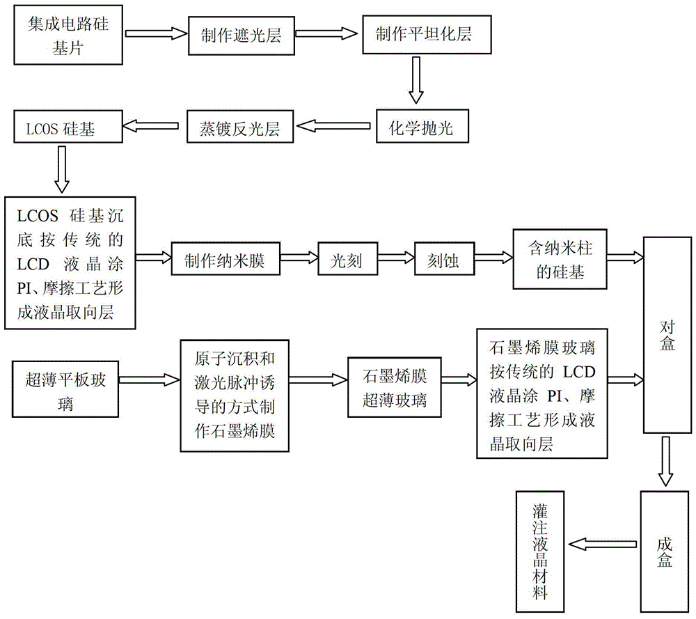

Image

  • A kind of lcos micro display device liquid crystal cell structure and manufacturing method thereof
  • A kind of lcos micro display device liquid crystal cell structure and manufacturing method thereof
  • A kind of lcos micro display device liquid crystal cell structure and manufacturing method thereof

Examples


Embodiment

[0050] Such as figure 2 As shown, a liquid crystal cell structure of a LCOS microdisplay device, the liquid crystal cell structure is a layered structure, including an electrode layer 1 on a graphene film, a liquid crystal material layer 2, a nano-column 3 and a silicon-based substrate layer 4, a silicon-based The substrate layer 4 is located in the lower layer, the upper electrode layer 1 is located in the upper layer, the liquid crystal material layer 2 and the nano column 3 are located in the middle layer, and the thickness of the liquid crystal cell can be adjusted by changing the height of the nano column 3 .

[0051] The main differences between the present invention and the prior art are:

[0052] 1. The upper electrode layer 1 is a graphene film flat glass.

[0053] The graphene film is used to replace the ITO film to improve the light transmittance, temperature stability and optical density of the light engine of the LCOS device. Introduce graphene technology, the ...


PUM

PropertyMeasurementUnit
thicknessaaaaaaaaaa
thicknessaaaaaaaaaa
transmittivityaaaaaaaaaa

Abstract

The invention relates to a liquid crystal box structure of a LCOS (Liquid Crystal on Silicon) micro display device and a manufacturing method of the liquid crystal box structure. The liquid crystal box structure is of a laminar structure, and comprises an upper electrode layer, a liquid crystal material layer, a nanorod and a silicon-based substrate layer, wherein the upper electrode layer is graphene film plate glass; the nanorod is a zinc oxide or titanium dioxide nanorod. The manufacturing method comprises the following steps: (A) preparing the silicon-based substrate layer; (B) preparing the nanorod on the silicon-based substrate layer to obtain a silicon-based substrate layer with the nanorod; (C) jointing the graphene film plate glass with the silicon-based substrate layer provided with the nanorod to assemble a liquid crystal box; (D) filling the liquid crystal box with a liquid crystal material to form a liquid crystal material layer. Compared with the prior art, the liquid crystal box structure has the advantages that the transmission is high, the thickness of a liquid crystal box is easy to control, and the working temperature can be up to 60 DEG C, so that the display performance of the device is greatly enhanced.

Description

technical field [0001] The invention relates to a microdisplay device, in particular to a structure of a liquid crystal box of an LCOS microdisplay device and a manufacturing method thereof. Background technique [0002] LCOS (Liquid Crystal on Silicon) is a relatively mature advanced technology. It is a new type of LCD display made on single crystal silicon, and it is an emerging technology that organically combines LCD and CMOS integrated circuits. LCOS has the characteristics of high resolution, reflective imaging, and low price. This technology first appeared in the late 1990s. Its first molded products were developed by Aurora Systems in 2000. Because the product has the characteristics of high resolution, high aperture ratio, and reflective imaging, it immediately attracted people's attention, and many companies began to conduct research and development. Among them are companies such as Sony, JVC, Canon, Intel, Philips, and UMC. [0003] The structural characteris...

Claims


Application Information

Patent Timeline
Patent Type & Authority Patents(China)
IPC IPC(8): G02F1/1333G02F1/1339
CPCG02F1/1333G02F1/13394G02F1/13398
Inventor 邢彦文马仁祥付敏恭李传南姚正钢付梦雨
Owner 上海长城计算机网络工程有限公司
Learn More