Liquid crystal display device

A technology of a liquid crystal display device and a liquid crystal layer, which is applied to static indicators, nonlinear optics, instruments, etc., and can solve problems such as the inability to obtain the suppression effect of flicker phenomenon and the inability to obtain the suppression effect of color shift phenomenon

Inactive Publication Date: 2015-01-14
MITSUBISHI ELECTRIC CORP
View PDF6 Cites 1 Cited by
  • Summary
  • Abstract
  • Description
  • Claims
  • Application Information

AI Technical Summary

Problems solved by technology

[0010] Therefore, if the method of disposing the slits is uniquely fixed, there is a problem that the effect of suppressing the flicker phenomenon cannot be obtained or the effect of suppressing the color shift phenomenon cannot be obtained depending on the driving method or the arrangement of the color materials.

Method used


Image

  • Liquid crystal display device
  • Liquid crystal display device
  • Liquid crystal display device

Examples


no. 1 Embodiment approach >

[0036]

[0037] As a first embodiment, an example of a liquid crystal display panel applied to an FFS (Fringe-Field Switching) mode will be described.

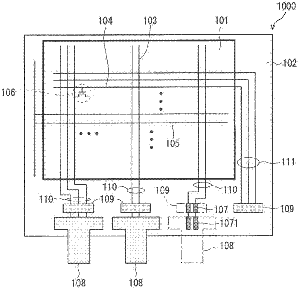
[0038] figure 1 It is a plan view showing the planar structure of the liquid crystal display panel 1000 according to this embodiment. In addition, the drawings are all schematic diagrams, and do not reflect the exact dimensions and the like of the structural elements shown. In addition, in order to avoid complexity, some structures are omitted or simplified.

[0039] Such as figure 1As shown, the liquid crystal display panel 1000 has a display area 101 for displaying images, and a frame area 102 provided to surround the display area 101 .

[0040] In the display area 101 , a plurality of signal lines 103 and a plurality of scanning lines 104 are arranged to intersect (orthogonally) each other. A portion where the signal line 103 intersects the scanning line 104 is referred to as an intersection. In addition, the plurali...

no. 2 Embodiment approach >

[0127]

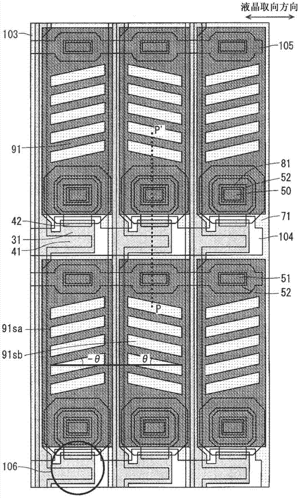
[0128] Figure 10 The arrangement of the TFTs 106 formed in the display region 101 in the TFT array substrate of the liquid crystal display device according to the second embodiment is shown.

[0129] exist Figure 4 In , one pixel is constituted by each having one gate wiring, one source wiring, and one TFT 106 , but in contrast, in Figure 10 In this case, two pixels are constituted by each having one gate wiring, two source wirings, and two TFTs 106 . In addition, if Figure 10 As shown, there are four kinds of arrangement positions of the TFT 106 in the pixel, forming an arrangement of 4×4 pixel periods.

[0130] Figure 11 is shown in the Figure 10 The TFTs 106 in the arrangement shown, and the liquid crystal display device having the color materials (RGBW) arranged in 2×2, the pixel polarity and the color material arrangement when performing column inversion driving.

[0131] The polarity of the pixel alternates positive (+) and negative (-) polarity in...


PUM


Abstract

The present invention includes first pixels formed to have a first slit having an inclination angle with respect to a rubbing direction and second pixels formed to have a second slit having an inclination angle opposite to the first slit, and at least one of the first pixels having a positive polarity allocated thereto and at least one of the first pixels having a negative polarity allocated thereto exist in the same frame, and at least one of the second pixels having the positive polarity allocated thereto and at least one of the second pixels having the negative polarity allocated thereto exist in the same frame.

Description

technical field [0001] The present invention relates to a liquid crystal display device, in particular to a liquid crystal display device which controls the alignment direction of liquid crystal molecules by using an electric field between electrodes disposed on the same substrate. Background technique [0002] As a method for widening the viewing angle of a liquid crystal display device, a lateral electric field is generated between electrodes disposed on the same substrate, and liquid crystal molecules are rotated in a plane parallel to the substrate by the electric field. As an example of using this method, an in-plane switching (In-plane Switching; hereinafter abbreviated as IPS) method or a fringe-field switching (Fringe-Field Switching; hereinafter abbreviated as FFS) method obtained by improving the IPS method is known. [0003] In the liquid crystal display device using the above method, the viewing angle is widened, but there is a problem in that the color change wh...

Claims


Application Information

Patent Timeline
Patent Type & Authority Applications(China)
IPC IPC(8): G02F1/1343
CPCG09G3/3648G02F1/134309G02F1/134363G02F1/134345G02F1/134372G09G3/3614G09G2300/0452G09G2310/0297
Inventor 奥本和范
Owner MITSUBISHI ELECTRIC CORP
Why Eureka
Try Eureka