Splicing structure of microscopic scattering dark field image on surface of optical element
A technology of microscopic scattering and optical components, which is used in image enhancement, image data processing, instruments, etc., and can solve the problems of long time stitching and poor robustness.
- Summary
- Abstract
- Description
- Claims
- Application Information
AI Technical Summary
Problems solved by technology
Method used
Image
Examples
Embodiment Construction
[0039] In order to make the object, technical solution and advantages of the present invention clearer, the present invention will be further described in detail below in conjunction with specific embodiments and with reference to the accompanying drawings.
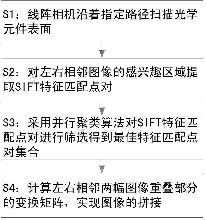
[0040] Figure 1A A flow chart showing a method for mosaicing microscopic scattering dark-field images on the surface of an optical element of the present invention includes the following steps:
[0041] Step S1: Use a line scan camera to scan the surface of the optical element along a specified path, and take a microscopic scattering dark field image of the surface of the optical element;
[0042] Step S2: extracting SIFT feature matching point pairs from the regions of interest of the left and right adjacent microscattering dark-field images;
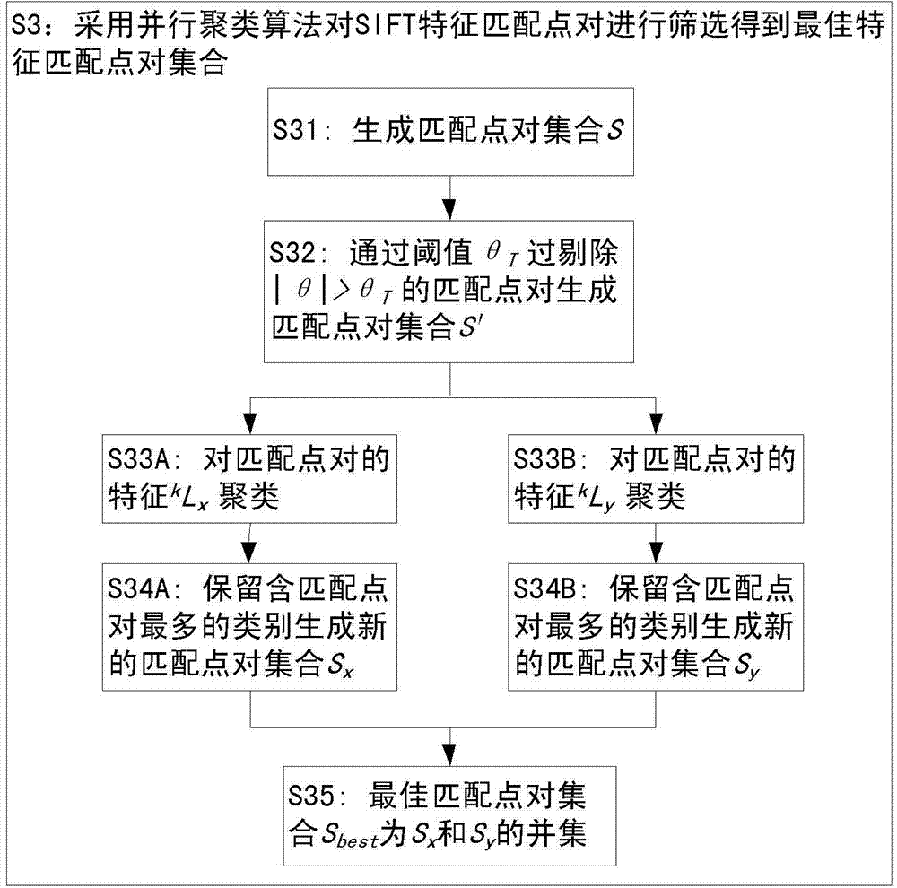
[0043] Step S3: Using a parallel clustering algorithm to filter the extracted SIFT feature matching point pairs to obtain the best set of feature matching point pairs;
[0044] ...
PUM
 Abstract
Description
Claims
Application Information
 - Generate Ideas
- Intellectual Property
- Life Sciences
- Materials
- Tech Scout
- Unparalleled Data Quality
- Higher Quality Content
- 60% Fewer Hallucinations
Browse by: Latest US Patents, China's latest patents, Technical Efficacy Thesaurus, Application Domain, Technology Topic, Popular Technical Reports.
© 2025 PatSnap. All rights reserved.Legal|Privacy policy|Modern Slavery Act Transparency Statement|Sitemap|About US| Contact US: help@patsnap.com


