
Pixel circuit as well as driving method and display device thereof

A pixel circuit and pixel structure technology, which is applied to circuits, electrical components, static indicators, etc., can solve problems such as difficult to achieve pixel resolution and increase pixel area, achieve high image quality, ensure uniformity, and improve The effect of flexibility

Active Publication Date: 2014-10-08
BOE TECH GRP CO LTD +1
View PDF6 Cites 50 Cited by
  • Summary
  • Abstract
  • Description
  • Claims
  • Application Information

AI Technical Summary

Problems solved by technology

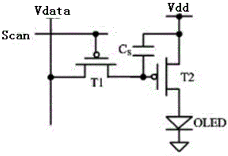
In the case of meeting the driving requirements, the number of multiple TFTs and Cs in the existing pixel circuit is affected by many factors such as the distribution space of TFT devices and TFT characteristics, it is difficult to use smaller TFTs to compress pixels, and it is difficult to achieve finer pixel resolution
[0006] At the same time, in the current field of touch electronics, capacitive touch and light-sensitive touch are the two most easily accepted and recognized by consumers. If the above two touch technologies can be integrated with OLED, the touch control process will Integrating with the OLED manufacturing process, these two represent the integration of high added value and the latest technology functions, and are bound to be in an unshakable position in the future display field
However, the increase of the above two touch functions will inevitably further increase the pixel area, making it more difficult to achieve fine pixel resolution

Method used


Image

  • Pixel circuit as well as driving method and display device thereof
  • Pixel circuit as well as driving method and display device thereof
  • Pixel circuit as well as driving method and display device thereof

Examples


Embodiment 1

[0063] This embodiment provides a pixel circuit and a corresponding driving method of the pixel circuit.

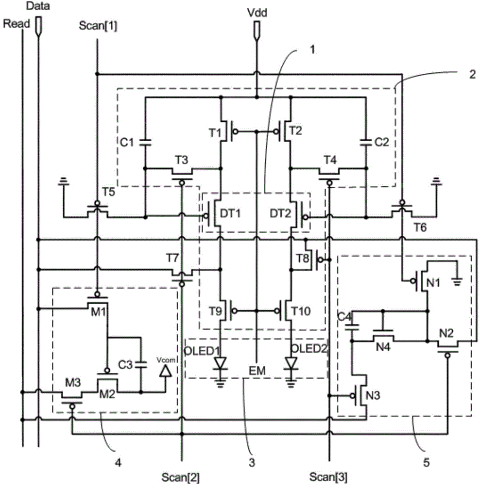
[0064] Such as image 3 As shown, a pixel circuit includes a plurality of pixel structures, and each pixel structure is equivalent to a sub-pixel unit. Wherein, the pixel structure includes a drive unit 1, a compensation unit 2, and a light emitting unit 3, wherein, in the adjacent first pixel structure and second pixel structure, the first pixel structure further includes a capacitive touch unit 4, and the second pixel structure further includes Including the photosensitive touch unit 5, and the compensation unit in the first pixel structure, the compensation unit in the second pixel structure, the capacitive touch unit 4, and the photosensitive touch unit 5 share a data line (Data Line), and the capacitive touch unit 4 It shares a read line (Read Line) with the light-sensitive touch unit 5 . in:

[0065] The compensation unit 2 is used to adjust the driving voltage o...

Embodiment 2

[0130] This embodiment provides a display device, including the pixel circuit in Embodiment 1.

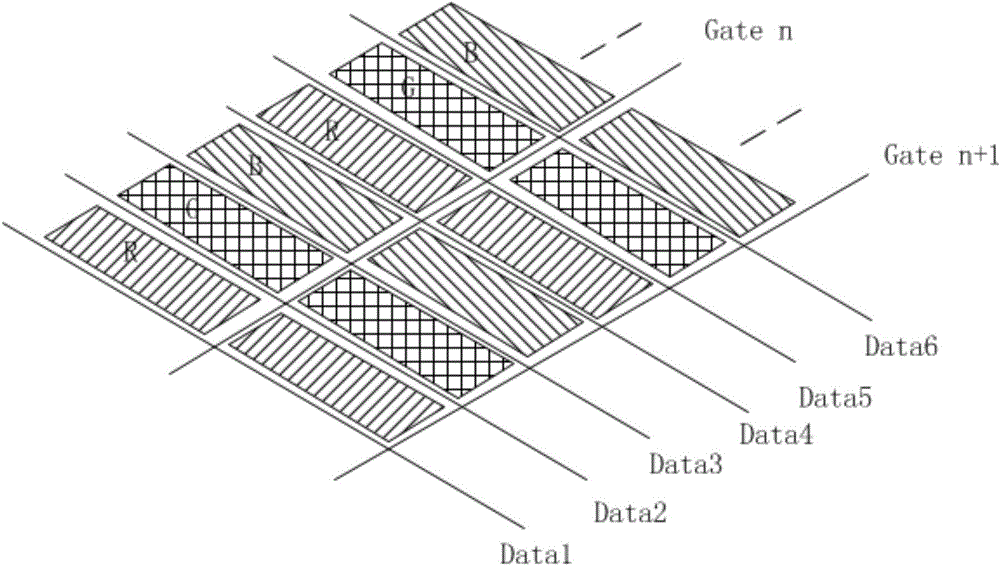
[0131] In the display device, including a plurality of pixel structures arranged in a matrix, the adjacent first pixel structure and the second pixel structure in the pixel circuit may be adjacent sub-pixel units of the same pixel unit, or may be adjacent different sub-pixel units. Neighboring sub-pixel units of the pixel unit. According to the pixel design in the display device, it can be designed according to actual needs such as Figure 6A The shown adjacent first pixel structure and the second pixel structure are pixel arrangements of adjacent sub-pixel units of the same pixel unit, or as Figure 6B The shown adjacent first pixel structure and second pixel structure are pixel arrangements of adjacent sub-pixel units of different adjacent pixel units.

[0132] Regardless of the above-mentioned arrangement, the compensation unit in the first pixel structure, the compensation un...


PUM


Abstract

The invention discloses a pixel circuit which comprises a plurality of pixel structures. Each pixel structure comprises a driving unit, a compensation unit and a light-emitting unit, wherein in the adjacent first pixel structure and second pixel structure, the first pixel structure further comprises a capacitance touch unit, the second pixel structure further comprises a light sensation touch unit, the compensation unit in the first pixel structure, the compensation unit in the second pixel structure, the capacitance touch unit and the light sensation touch unit share a data line, and the capacitance touch unit and the light sensation touch unit share a read line. The pixel circuit integrates the capacitance touch function and the light sensation touch function, and the touch flexibility is improved; and the compensation units, the capacitance touch unit and the light sensation touch unit share the data line, and the capacitance touch unit and the light sensation touch unit share the read line, pixel sizes can be reduced substantially, the IC cost is reduced, current flowing through an OLED in each pixel can be free from the effect of Vth, and finally the image display uniformity is guaranteed.

Description

technical field [0001] The invention belongs to the field of display technology, in particular to a pixel circuit and its driving [0002] Method, display device. Background technique [0003] Organic light-emitting diode (Organic Light-Emitting Diode, referred to as OLED) display device is one of the hot spots in the field of flat panel display research. Compared with liquid crystal display (Liquid Crystal Display, referred to as LCD), OLED has low energy consumption and low production cost. , self-illumination, wide viewing angle and fast response. At present, OLEDs have gradually replaced traditional LCDs in display fields such as mobile phones, PDAs, and digital cameras. [0004] In OLED technology, pixel drive circuit design is the core technical content. LCD is voltage-driven, which uses a stable voltage to control the light transmission brightness of liquid crystals; unlike LCD, OLED is current-driven and requires a stable current to control the OLED device to emit...

Claims


Application Information

Patent Timeline
Patent Type & Authority Applications(China)
IPC IPC(8): G09G3/32G09G3/3233
CPCG09G3/3233G09G2310/0262G09G2360/14G06F3/0412G06F2203/04105G06F3/042G06F3/044G09G2300/0804G06F3/04184H10K59/40G06F3/04166
Inventor 杨盛际
Owner BOE TECH GRP CO LTD
Learn More