
Organic silica gel die-free encapsulation method for circuit board assembly

A circuit board component and silicone technology, applied in the direction of electrical components, printed circuits, printed circuit manufacturing, etc., can solve the problems that are not conducive to small batches and multi-variety products, the processing time occupied by potting molds, and the increase in processing costs. To achieve the effect of flexible method, low cost and short production cycle

Active Publication Date: 2014-09-10
BEIJING HUAHANG RADIO MEASUREMENT & RES INST
View PDF4 Cites 9 Cited by
  • Summary
  • Abstract
  • Description
  • Claims
  • Application Information

AI Technical Summary

Problems solved by technology

The design and production of potting molds take up a certain amount of processing time and increase processing costs, especially not conducive to small batches and multi-variety products

Method used


Image

  • Organic silica gel die-free encapsulation method for circuit board assembly
  • Organic silica gel die-free encapsulation method for circuit board assembly

Examples


Embodiment

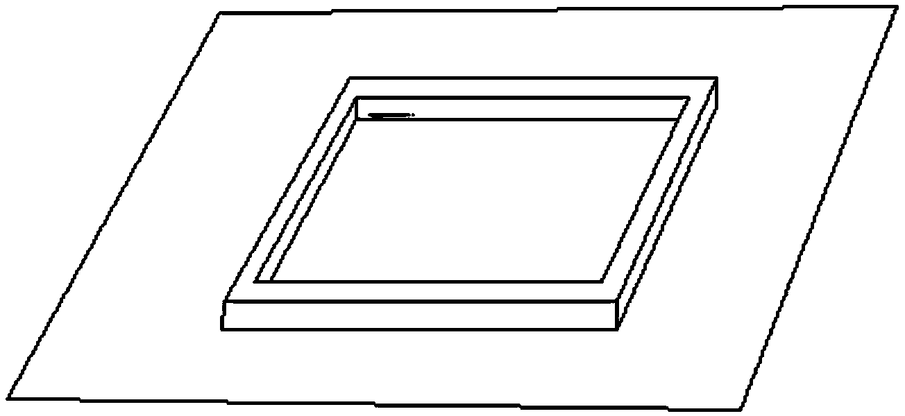
[0058] A certain circuit board assembly requires the CS surface to be potted with GN521 silicone gel. The circuit board is a rectangle of 80mm×120mm. There are no components within 4mm of the circuit board side, and the thickness of the adhesive layer is required to be 3.5mm. The specific implementation process of circuit board potting is:

[0059] Strip production:

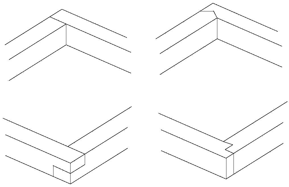
[0060] The thickness of the glue-filling layer is required to be 3.5mm. Due to the effect of surface tension, the glue liquid climbs up about 0.5mm before curing near the mold, so it is necessary to make a 4mm-high glue strip; there are no components within 4mm from the edge of the circuit board. In order for the adhesive strip to be stably fixed on the circuit board, the thickness of the adhesive strip should be as thick as possible. Set the thickness of the adhesive strip to 3mm. After the adhesive strip is fixed on the circuit board, there is still a margin of about 1mm on the edge of the circuit board, which ...


PUM


Abstract

The invention discloses an organic silica gel die-free encapsulation method for a circuit board assembly. According to the method, pre-cured organic silica gel is cut into gel tapes with proper dimensions, the gel tapes enclose an encapsulation area and are fixed on a circuit board, and encapsulation can be carried out after leaking stoppage; the gel tapes can be reserved or removed according to actual conditions after the encapsulation. The method disclosed by the invention is capable of designing and producing a special encapsulation die as a substitute, reducing cost and shortening period, and especially suitable for small-batch and multi-variety products.

Description

technical field [0001] The invention relates to a sealing and potting method, in particular to a silicone gel potting process method for a circuit board component, which can complete partial or overall potting of the circuit board component without making a special potting mold. Background technique [0002] Potting process technology uses insulating medium to exclude air and fill it around components to achieve reinforcement and improve the electrical strength of components. It is a commonly used protection process method for circuit board components. For example, when working outdoors, the circuit boards outside the cabin of the ship need to be potted to prevent moisture, condensation, and salt spray from corroding the circuit; in order to improve the three-proof performance of electronic equipment working at sea, all Transformers and choke coils require potting, wrapping, encapsulation or end sealing; in order to improve the anti-vibration capability of airborne and aeros...

Claims


Application Information

Patent Timeline
Patent Type & Authority Applications(China)
IPC IPC(8): H05K3/00
Inventor 刘晓玲徐婷安宏奇
Owner BEIJING HUAHANG RADIO MEASUREMENT & RES INST
Learn More