
amoled pixel test circuit

A technology for testing circuits and pixels, applied in static indicators, instruments, etc., can solve problems such as increasing the cost of supporting equipment, and achieve the effect of reducing the number of independent probes and reducing costs

Active Publication Date: 2016-10-05
EVERDISPLAY OPTRONICS (SHANGHAI) CO LTD
View PDF6 Cites 0 Cited by
  • Summary
  • Abstract
  • Description
  • Claims
  • Application Information

AI Technical Summary

Problems solved by technology

[0006] Moreover, as the complexity of the circuit increases, the number of independent probes required may increase accordingly. Therefore, it may be necessary to equip the measuring machine with more independent probes to complete relevant measurements.
As a result, the cost of supporting equipment will increase

Method used


Image

  • amoled pixel test circuit
  • amoled pixel test circuit
  • amoled pixel test circuit

Examples


Embodiment Construction

[0023] Hereinafter, embodiments of the present invention will be described in detail with reference to the drawings.

[0024] In the following drawings, the same reference numerals are attached to the same or corresponding parts, and repeated descriptions will be omitted.

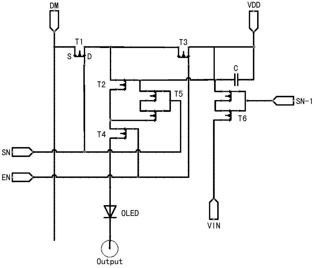
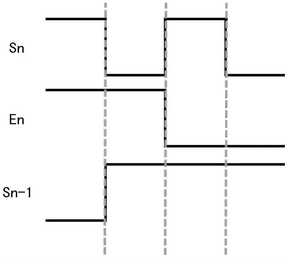
[0025] figure 2 yes means figure 1 The timing waveform diagram of the lighting control signal, the current scan signal and the front row scan signal of the pixel test circuit shown.

[0026] Such as figure 2 As shown, when the current scanning signal SN and the light-emitting control signal EN are both high level 1, the front row scanning signal SN-1 is low-level 0; when the current scanning signal SN is low-level 0, the light-emitting control signal EN is When the high level is 1, the front row scanning signal SN-1 is high level 1; when the current scanning signal SN is high level 1 and the light control signal EN is low level 0, the front row scanning signal SN-1 is high Level 1; when the current sc...


PUM


Abstract

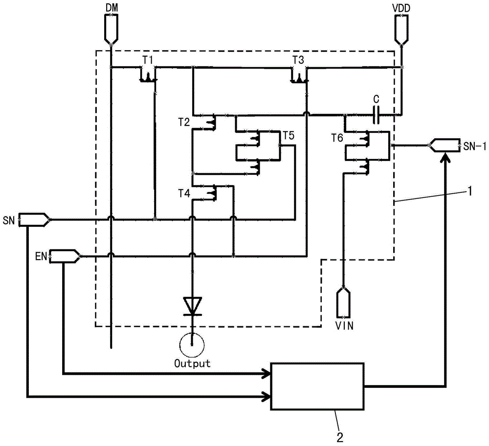
The present invention provides an AMOLED pixel testing circuit, which includes a pixel driving module and an NAND logic circuit module; the pixel driving circuit is connected with a power supply terminal, a data signal terminal, a current scanning signal terminal, a front row scanning signal terminal, a preset Voltage terminal, light emission control signal input terminal and output terminal; the above-mentioned NAND logic circuit module uses the signal of the light emission control signal input terminal of the above-mentioned pixel driving module and the signal of the current scanning signal input terminal as input signals, and the output terminal of the above-mentioned NAND logic circuit module Connect to the front-row scan signal input terminal of the above-mentioned pixel driving module. According to the AMOLED pixel testing circuit of the present invention, when using the TEG measuring machine for measurement, it is not necessary to measure the signal at the input terminal of the scanning signal in the front row, thus reducing the number of independent probes required for the measurement.

Description

technical field [0001] The invention relates to an AMOLED pixel test circuit, in particular to an AMOLED pixel test circuit which reduces the number of probes required for measurement. Background technique [0002] AMOLED (Active Matrix / Organic Light Emitting Diode: Active Matrix Organic Light Emitting Diode panel) is called the next generation display technology due to its faster response speed, higher contrast ratio, and wider viewing angle. [0003] In the current AMOLED products, the pixel circuit in the AA area generally adopts nTmC (n≥4, m≥1, m and n are positive Integer) structure, its circuit design is more complicated. Therefore, the process requirements are more stringent when designing high-resolution products. In order to monitor the product more timely and accurately, a test circuit (testkey) with test points corresponding to each component is usually set in the AMOLED product, and the parameters of each component are obtained by measuring each test circuit. ...

Claims


Application Information

Patent Timeline
Patent Type & Authority Patents(China)
IPC IPC(8): G09G3/3225G09G3/00
Inventor 董杭孙鲁男左文霞柯其勇
Owner EVERDISPLAY OPTRONICS (SHANGHAI) CO LTD
Learn More