Array substrate of electronic paper, manufacturing method thereof and electronic paper

A technology of an array substrate and a manufacturing method, which is applied in the display field and can solve problems affecting the performance of electronic paper, etc.

Active Publication Date: 2014-08-06
BOE TECH GRP CO LTD +1
View PDF5 Cites 7 Cited by
  • Summary
  • Abstract
  • Description
  • Claims
  • Application Information

AI Technical Summary

Problems solved by technology

However, the current electronic paper does not have the function of touch, which affects the performance of electronic paper

Method used


Image

  • Array substrate of electronic paper, manufacturing method thereof and electronic paper
  • Array substrate of electronic paper, manufacturing method thereof and electronic paper
  • Array substrate of electronic paper, manufacturing method thereof and electronic paper

Examples


Embodiment Construction

[0066] Specific embodiments of the present invention will be described in detail below in conjunction with the accompanying drawings. It should be understood that the specific embodiments described here are only used to illustrate and explain the present invention, and are not intended to limit the present invention.

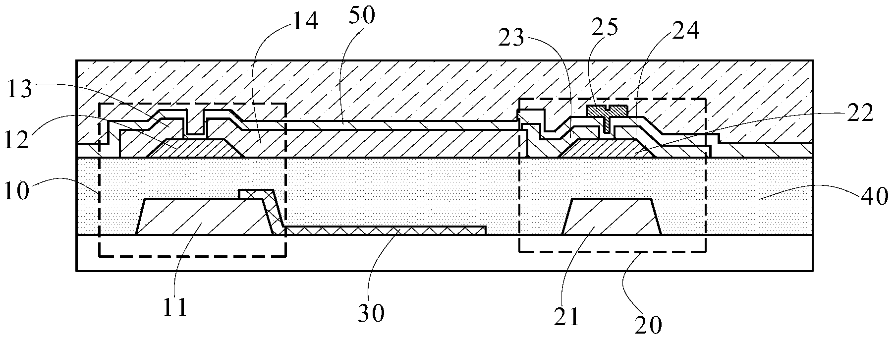
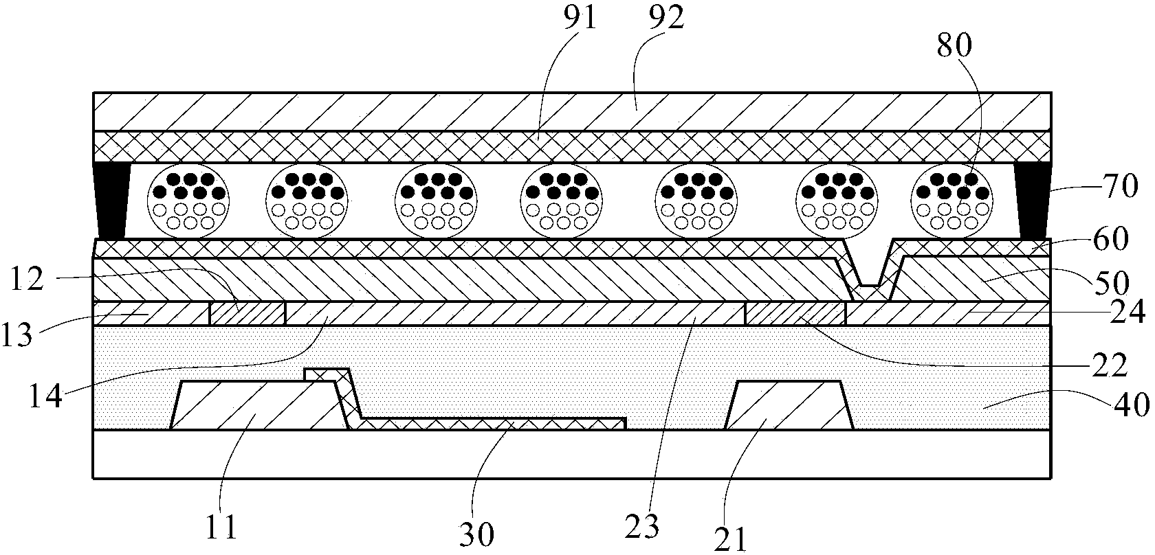
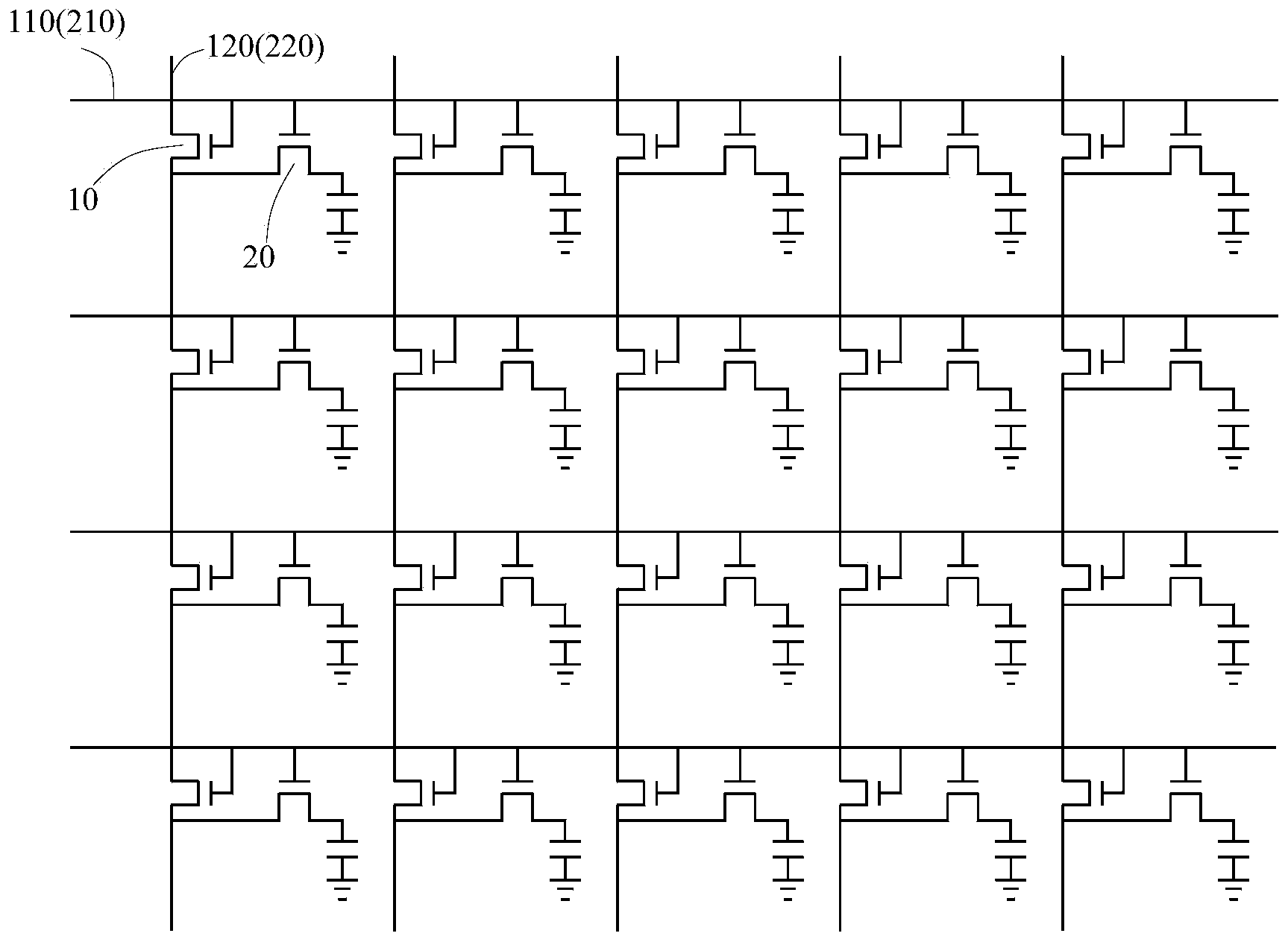
[0067] As an aspect of the present invention, such as Figure 1 to Figure 3 As shown in , an array substrate for electronic paper is provided, wherein the array substrate includes a plurality of signal emission lines 110, a plurality of sensing signal lines 120 and a plurality of photosensitive thin film transistors 10, and the source electrodes of the photosensitive thin film transistors 10 and the drain are arranged on the sensing signal line 120, the signal emission line 110 is connected to the gate of the photosensitive thin film transistor 10, and the position of the active layer 12 of the photosensitive thin film transistor is between two adjacent electron...


PUM


Abstract

The invention provides an array substrate used for electronic paper. The array substrate comprises a plurality of signal emission lines, a plurality of sensing signal lines and a plurality of photosensitive thin film transistors, wherein the source electrodes and the drain electrodes of the photosensitive thin film transistors are arranged on the sensing signal lines, the signal emission lines are connected with the grid electrodes of the photosensitive thin film transistors, and an active layer of each photosensitive thin film transistor corresponds to the gap between every two adjacent points of electronic ink in the electronic paper in position. The invention further provides a manufacturing method of the array substrate and the electronic paper comprising the array substrate. The photosensitive thin film transistors are additionally arranged on the array substrate of the electronic paper, so that touch and control operation on the electronic paper is achieved.

Description

technical field [0001] The present invention relates to the field of display technology, in particular, to an array substrate of electronic paper, a manufacturing method thereof, and an electronic paper including the array substrate. Background technique [0002] Existing electronic paper generally includes an array substrate and a transparent electrode substrate facing each other, and electronic ink arranged between the array substrate and the transparent substrate. Thin film transistors are arranged on the array substrate, and the thin film transistors control the electric field between the pixel electrodes and the common electrodes. When the electric field is negative, the white ions in the e-ink are shown above, and when the electric field is positive, the black ions in the e-ink are shown above. However, the current electronic paper does not have a touch function, which affects the performance of the electronic paper. [0003] Therefore, how to enable the electronic p...

Claims


Application Information

Patent Timeline
Patent Type & Authority Applications(China)
IPC IPC(8): H01L27/12H01L21/77G06F3/041
Inventor 田宗民张金中谢振宇
Owner BOE TECH GRP CO LTD
Why Eureka
Try Eureka