Method and device for pcb puzzle

A special-shaped board and sliding direction technology, which is applied in the direction of assembling printed circuits with electrical components, computer-designed circuits, and simultaneous processing of multiple printed circuits, can solve the problem of low utilization of boards, reduce production materials, reduce costs, The effect of improving computational efficiency

Active Publication Date: 2017-10-31
SHENZHEN PARTNER INFORMATION TECH
View PDF1 Cites 0 Cited by
  • Summary
  • Abstract
  • Description
  • Claims
  • Application Information

AI Technical Summary

Problems solved by technology

In the case that the Pcs that need to be assembled are special-shaped boards, but their positions in the Set are fixed, so that the utilization rate of the Set's boards is usually low

Method used


Image

  • Method and device for pcb puzzle
  • Method and device for pcb puzzle
  • Method and device for pcb puzzle

Examples


Embodiment Construction

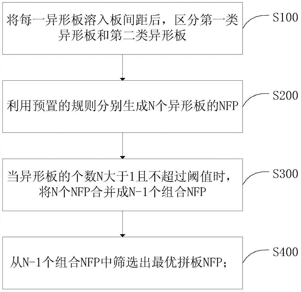
[0034] In order to make the object, technical solution and advantages of the present invention more clear, the present invention will be further described in detail below in conjunction with the accompanying drawings and embodiments. It should be understood that the specific embodiments described here are only used to explain the present invention, not to limit the present invention.

[0035] Embodiments of the present invention relate to a panelizing method used in cutting PCB materials, and in particular to a panelizing method for special-shaped boards.

[0036] Please refer to figure 1 , is the PCB puzzle method proposed by the embodiment of the present invention, such as figure 1 As shown, the method includes the following steps:

[0037] S100: After dissolving each special-shaped board into the board spacing, distinguish the first type of special-shaped board from the second type of special-shaped board;

[0038] Wherein, the first type of special-shaped board is a spe...


PUM


Abstract

A PCB splicing method and device. The method comprises: after sketch plates are integrated into plate gaps, distinguishing sketch plates of a first type and sketch plates of a second type; respectively generating sketch plate no-fit polygons (NFPs)according to a pre-set rule, wherein the sketch plates of the first type generate sketch plate NFPs in corresponding rectangles, and the sketch plates of the second type generate sketch plate NFPs on original sketch plates; when the number N of the sketch plates is greater than 1 and does not exceed a threshold value, combining the N NFPs in pairs to generate N sketch plate combination patterns; and screening out an optimal splicing combination pattern from the N sketch plate combination patterns. The sketch plates which are already integrated into the plate gaps are combined so as to generate and screen out the optimal place splicing combination pattern by means of a combination process using the pre-set rule, and in the combination process, sketch plates which conform to requirements are converted into rectangles for processing, thereby improving the PCB production efficiency and the combination-method calculation efficiency, reducing the production materials of the sketch plates, and reducing the costs.

Description

technical field [0001] The invention relates to the technical field of PCB (Printed Circuit Board, printed circuit board), in particular to a PCB splicing method and device. Background technique [0002] At present, when it is necessary to combine multiple PCB products of the same process, it is usually used to manually combine multiple Pcs (the smallest shipment unit of a class of PCB products) into a Set (the smallest unit of production, which is determined by the Pcs synthesis). In the case that the Pcs that need to be assembled are special-shaped boards, but their positions in the Set are fixed, so that the utilization rate of the boards in the Set is usually low. Contents of the invention [0003] The main purpose of the present invention is to provide a method and device for PCB splicing, aiming at reducing the production material cost of PCB special-shaped splicing and quickly generating a splicing plan. [0004] In order to achieve the above object, the present i...

Claims


Application Information

Patent Timeline
Patent Type & Authority Patents(China)
IPC IPC(8): H05K3/36
CPCH05K3/0097H05K3/0005
Inventor 曾宪雄
Owner SHENZHEN PARTNER INFORMATION TECH
Why Eureka
Try Eureka