Junction terminal structure of transverse high-voltage power semiconductor device
A power semiconductor, lateral high voltage technology, applied in semiconductor devices, electrical components, circuits, etc., can solve problems such as depletion, achieve the effect of optimizing withstand voltage, ensuring withstand voltage, and increasing process steps and costs
- Summary
- Abstract
- Description
- Claims
- Application Information
AI Technical Summary
Problems solved by technology
Method used
Image
Examples
Embodiment 1
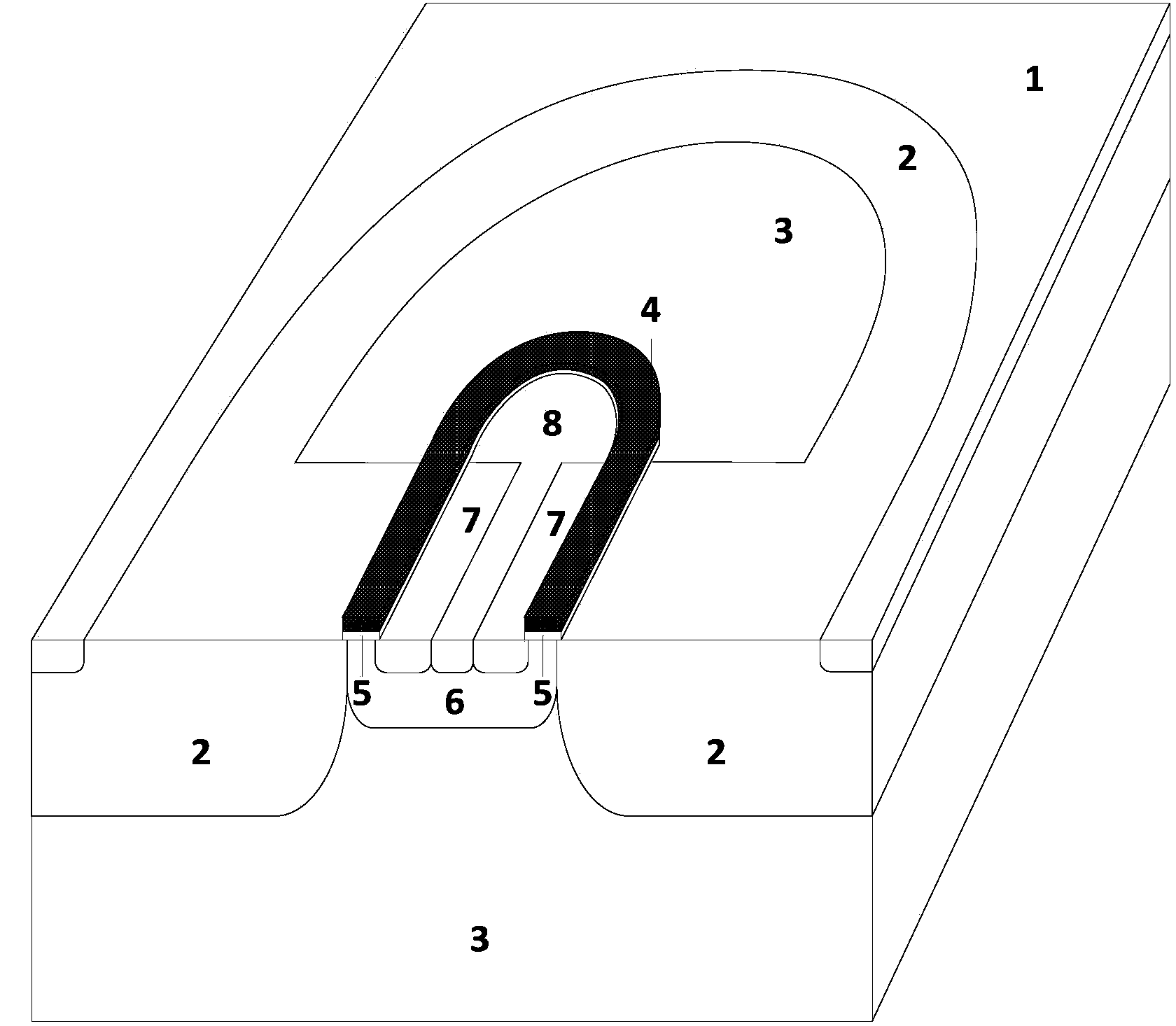
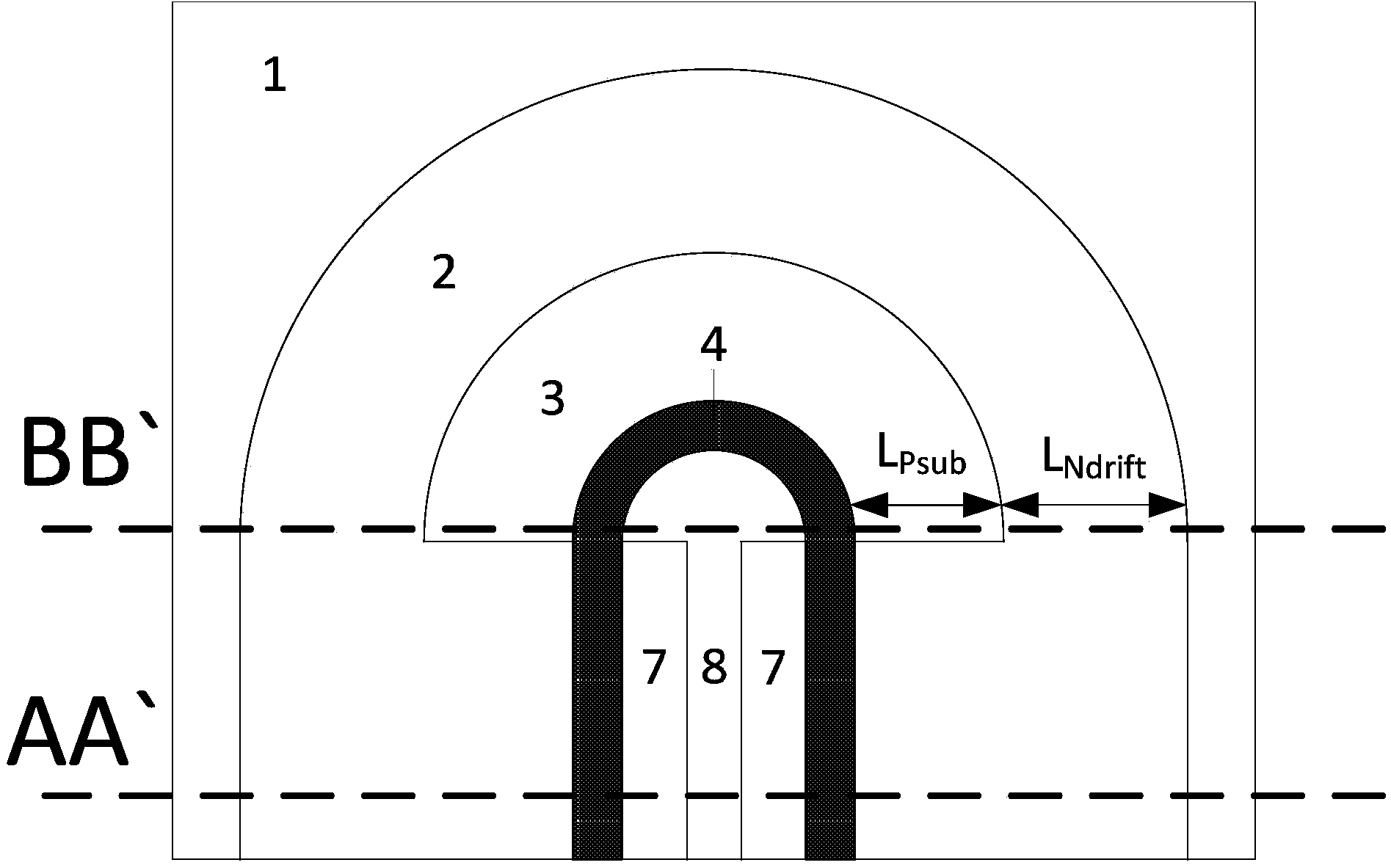
[0029] Such as Figure 10 As shown, this example includes a straight line junction termination structure and a curvature junction termination structure; the straight junction termination structure is the same as the active region structure of a lateral high-voltage power semiconductor device, including the drain N +Contact region 1, N-type drift region 2, P-type substrate 3, gate polysilicon 4, gate oxide layer 5, P-well region 6, source N + Contact area 7, source P + Contact region 8; P-well region 6 and N-type drift region 2 are located on the upper layer of P-type substrate 3, wherein P-well region 6 is located in the middle, with N-type drift region 2 on both sides, and P-well region 6 and N-type drift region 2 The drift region 2 is connected; the two sides of the N-type drift region 2 away from the P-well region 6 are the drain N + Contact area 1; drain N + The lateral width of the end of the contact region 1 away from the curvature junction terminal structure is great...
Embodiment 2
[0033] Such as Figure 11 As shown, the difference between this example and Example 1 is that the original L of the device at the terminal of the curvature junction is kept Ndriftt In the case of the same length, the increase of L Psub length, becomes L Psub +ΔL, thereby increasing the area of the P-type substrate region. When the substrate doping concentration is low, the depletion region will soon extend to the P-type substrate region. At this time, increasing the area of the P-type substrate region can prevent the P The type substrate region is depleted in advance to ensure the withstand voltage of the device at the curvature junction terminal.
Embodiment 3
[0035] Such as Figure 12 As shown, the difference between this example and Example 1 is that while increasing L Psub length and L Ndrift length, making it L Psub +ΔL 1 and L Ndrift +ΔL 2 , where ΔL 1 with ΔL 2 The sum is equal to ΔL, thereby increasing the area of the P-type substrate region and the N-type drift region at the same time, so that the withstand voltage of the device can be optimized.
PUM
 Abstract
Description
Claims
Application Information
 - R&D Engineer
- R&D Manager
- IP Professional
- Industry Leading Data Capabilities
- Powerful AI technology
- Patent DNA Extraction
Browse by: Latest US Patents, China's latest patents, Technical Efficacy Thesaurus, Application Domain, Technology Topic, Popular Technical Reports.
© 2024 PatSnap. All rights reserved.Legal|Privacy policy|Modern Slavery Act Transparency Statement|Sitemap|About US| Contact US: help@patsnap.com


