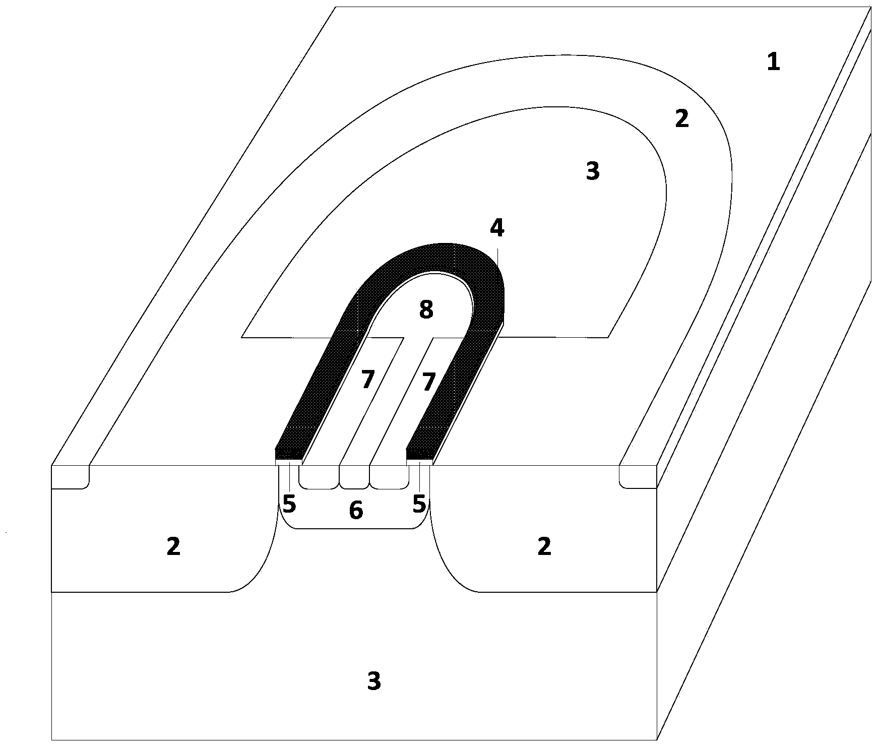
Junction terminal structure of transverse high-voltage power semiconductor device
A technology of power semiconductors and lateral high voltage, applied in the direction of semiconductor devices, electrical components, circuits, etc., can solve problems such as breakdown, achieve the effect of improving withstand voltage, ensuring withstand voltage, increasing process steps and cost
- Summary
- Abstract
- Description
- Claims
- Application Information
AI Technical Summary
Problems solved by technology
Method used
Image
Examples
Embodiment 1
[0030] Such as Figure 10 As shown, this example includes a linear junction terminal structure and a curvature junction terminal structure; the linear junction terminal structure is the same as the active region structure of a lateral high-voltage power semiconductor device, including the drain N + Contact region 1, N-type drift region 2, P-type substrate 3, gate polysilicon 4, gate oxide layer 5, P-well region 6, source N + Contact area 7, source P + Contact region 8; P-well region 6 and N-type drift region 2 are located on the upper layer of P-type substrate 3, wherein P-well region 6 is located in the middle, with N-type drift region 2 on both sides, and P-well region 6 and N-type drift region 2 The drift region 2 is connected; the two sides of the N-type drift region 2 away from the P-well region 6 are the drain N + Contact region 1, the upper layer of P-well region 6 has a source N connected to the metallized source + contact area 7 and the source P + contact region 8...
Embodiment 2
[0034] Such as Figure 11 As shown, the difference between this example and Example 1 is that the original L of the device at the terminal of the curvature junction is kept Psub In the case of the same length, the increase of L Ndrift length, becomes L Ndrift +ΔL, thereby increasing the area of the N-type drift region. The working principle of this example is: when the substrate doping concentration is high, the area of the N-type drift region can be appropriately increased, so that the P-type substrate and the N-type The withstand voltage of the drift region reaches the maximum.
Embodiment 3
[0036] Such as Figure 12 As shown, the difference between this example and Example 1 is that while increasing L Psub length and L Ndrift length, making it L Psub +ΔL 1 and L Ndrift +ΔL 2 , where ΔL 1 with ΔL 2 The sum is equal to ΔL, thereby increasing the area of the P-type substrate region and the N-type drift region at the same time, so that the withstand voltage of the device can be optimized.
PUM
 Abstract
Description
Claims
Application Information
 - R&D
- Intellectual Property
- Life Sciences
- Materials
- Tech Scout
- Unparalleled Data Quality
- Higher Quality Content
- 60% Fewer Hallucinations
Browse by: Latest US Patents, China's latest patents, Technical Efficacy Thesaurus, Application Domain, Technology Topic, Popular Technical Reports.
© 2025 PatSnap. All rights reserved.Legal|Privacy policy|Modern Slavery Act Transparency Statement|Sitemap|About US| Contact US: help@patsnap.com


