High-resolution test device for transistor characteristic curve tracer

A technology for transistor characteristics and testing devices, applied in measuring devices, single semiconductor device testing, instruments, etc., can solve problems such as the influence of capacitive current measurement results, the influence of contact resistance and lead resistance voltage measurement results, etc.

Inactive Publication Date: 2014-06-04
JIANGSU LVYANG ELECTRONICS INSTR GROUP
View PDF2 Cites 4 Cited by
  • Summary
  • Abstract
  • Description
  • Claims
  • Application Information

AI Technical Summary

Problems solved by technology

[0002] The measurement circuit used by the current transistor characteristic parameter test instrument has an influence on the high-resolution current measurement result of the ADC during the small current test; the influence of contact resistance and lead resistance on the voltage measurement result during the high current test

Method used


Image

  • High-resolution test device for transistor characteristic curve tracer
  • High-resolution test device for transistor characteristic curve tracer

Examples


Embodiment Construction

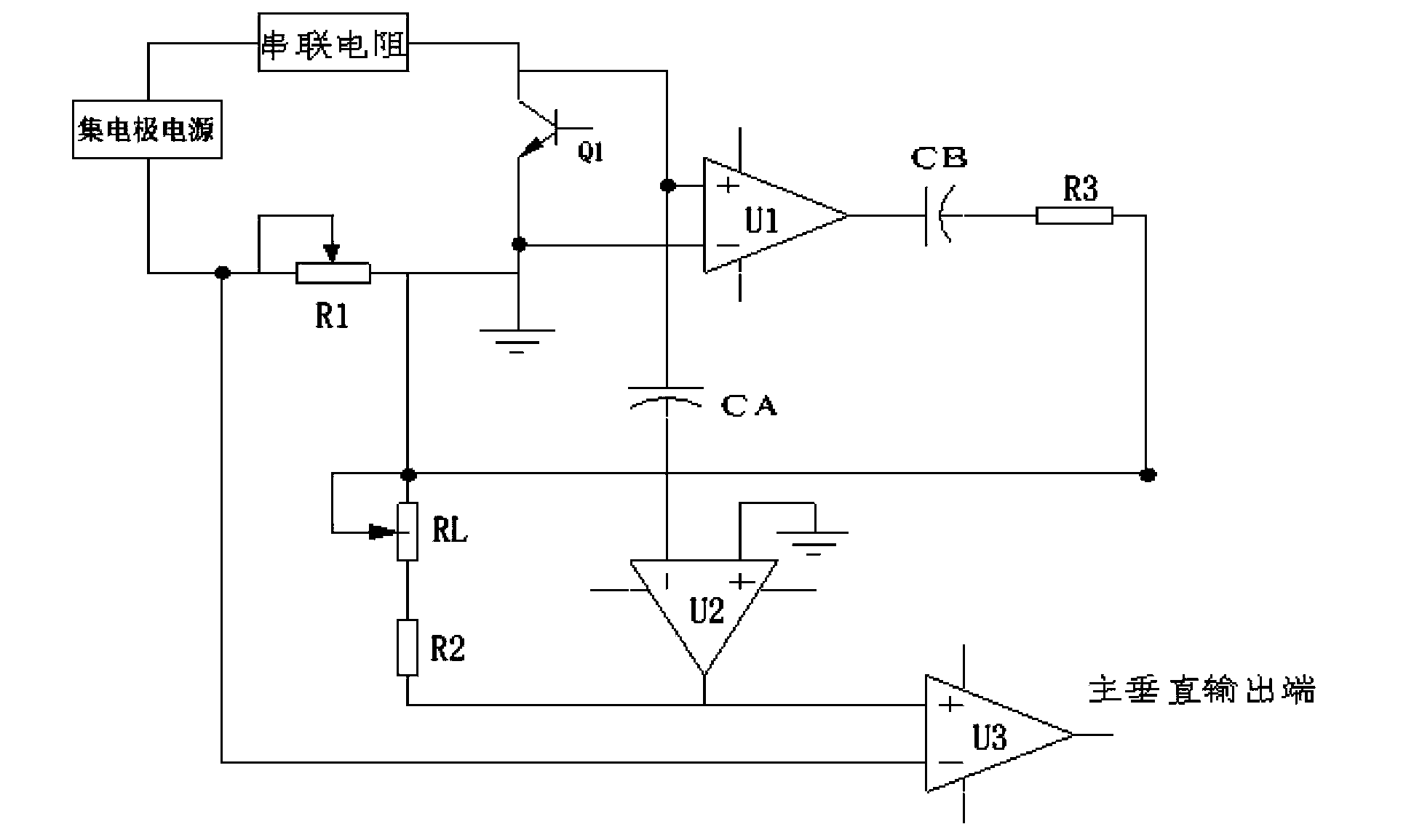
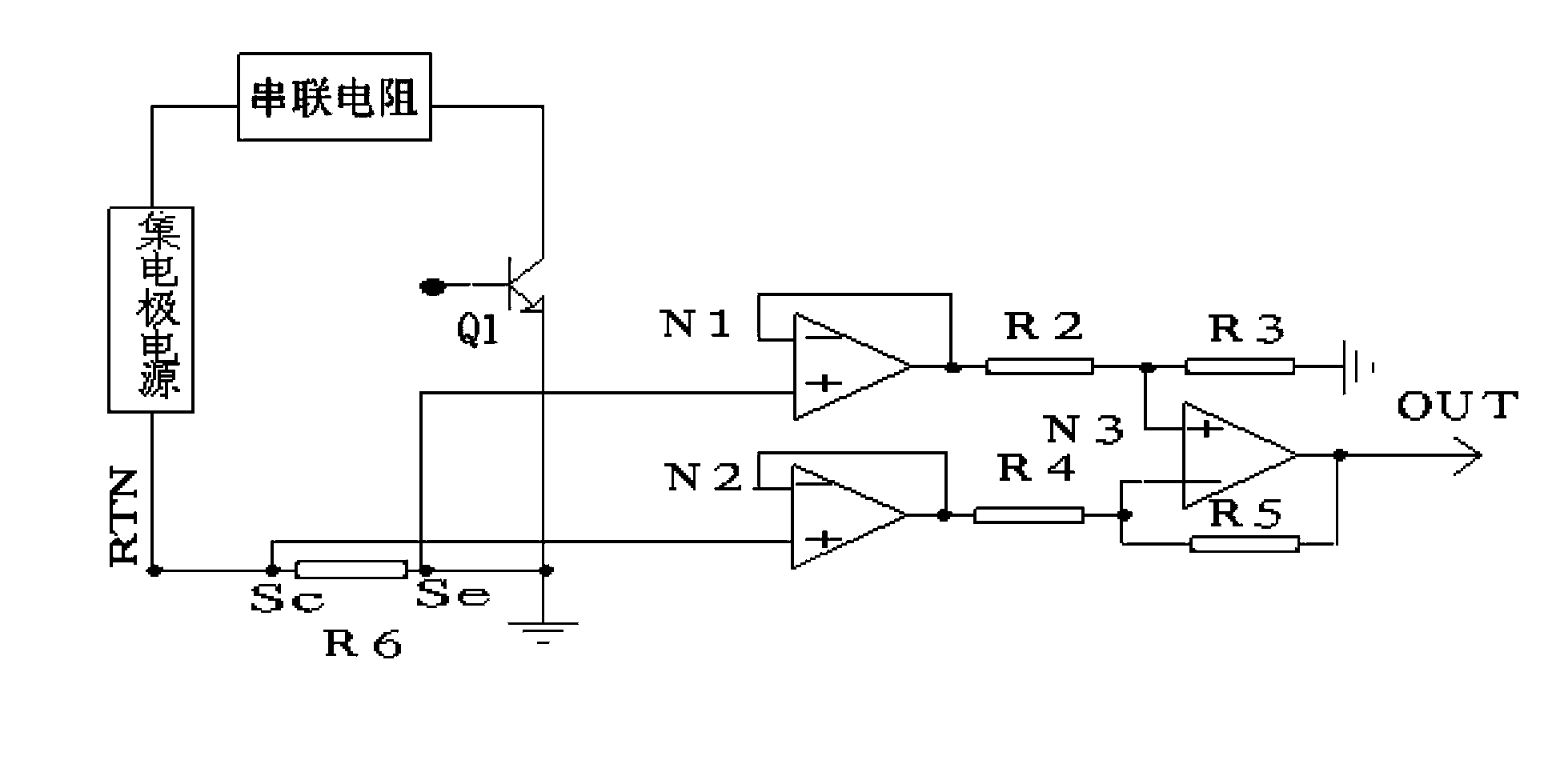
[0011] The high-resolution test device of the transistor characteristic graphing instrument of the present invention comprises the triode Q1 of the test piece, the collector of the triode Q1 is connected in series with a series resistor and a collector power supply in sequence, and a capacitive current is provided between the collector power supply and the emitter of the triode Q1 Compensation device or sampling loop high-resolution differential amplifier.

[0012] The capacitive current compensation device includes a current sampling resistor R1, an operational amplifier U1, an operational amplifier U2, a differential amplifier U3, a capacitor CA, a capacitor CB, a resistor R2, a resistor R3, and a compensation resistor RL. The current sampling resistor R1 is set between the collector power supply and Between the emitters of the transistor Q1, one end of the current sampling resistor R1 is respectively connected to the negative input terminal of the operational amplifier U1 an...


PUM


Abstract

The invention provides a parameter measurement device and especially relates to the transistor characteristic curve tracer high-resolution test technology. A high-resolution test device for a transistor characteristic curve tracer comprises a measured piece triode Q1. The collector of the triode Q1 is sequentially connected with a series resistor and a collector power supply in series. A capacitive current compensation device or a sampling loop high-resolution differential amplification device is arranged between the collector power supply and the emitter of the triode Q1. The highly-sensitive differential amplification and compensation circuits are utilized to prevent the influence of a capacitive current in small current testing, and prevent the voltage drop due to contact resistance and lead resistance from being collected by a voltage sampling circuit in the large current testing, so that in the voltage measurement, an ADC high-resolution test result can be obtained.

Description

technical field [0001] The invention proposes a parameter measuring device, in particular to a high-resolution testing technology of a transistor characteristic graph instrument. Background technique [0002] The measurement circuit used by the current transistor characteristic parameter testing instrument has an influence on the high-resolution current measurement results of the ADC when the capacitive current is used in the small current test; there is an influence on the voltage measurement result by the contact resistance and the lead resistance in the high current test. How to realize the high precision of ADC depends on the measurement circuit technology. Contents of the invention [0003] The technical effects of the present invention can overcome the above-mentioned defects, and provide a high-resolution transistor graph test device, which can realize ADC high-precision measurement results. [0004] In order to achieve the above object, the present invention adopt...

Claims


Application Information

Patent Timeline
Patent Type & Authority Applications(China)
IPC IPC(8): G01R31/26G01R1/30
Inventor 刘礼伟宋云衢
Owner JIANGSU LVYANG ELECTRONICS INSTR GROUP
Why Eureka
Try Eureka