PCB expansion and contraction compensation method
A technology of PCB board and compensation method, applied in electrical components, printed circuit components, printed circuit manufacturing, etc., can solve the problems of low PCB board accuracy and large deviation of PCB board expansion and shrinkage.
- Summary
- Abstract
- Description
- Claims
- Application Information
AI Technical Summary
Problems solved by technology
Method used
Image
Examples
Embodiment Construction
[0020] Embodiments of the present invention are described in detail below in conjunction with accompanying drawings:
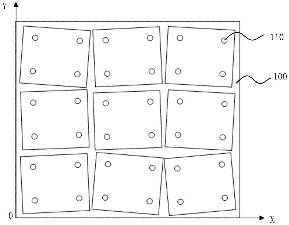
[0021] like figure 1 Shown, a kind of PCB expansion and contraction compensation method comprises the following steps:
[0022] S100: Divide the PCB board into multiple areas;
[0023] S200: setting at least two reference targets on each area;
[0024] S300: Measure the actual position of the reference target on each area after pressing the PCB board, compare it with the theoretical position, and convert the expansion and contraction values of each area;
[0025] S400: According to the expansion and contraction values of each area, perform partition compensation for each subsequent process.
[0026] The above PCB board expansion and contraction compensation method divides the PCB board before lamination into multiple areas, and sets at least two reference targets on each area, measures the actual position of the reference target on each area of the PC...
PUM
 Abstract
Description
Claims
Application Information
 - R&D
- Intellectual Property
- Life Sciences
- Materials
- Tech Scout
- Unparalleled Data Quality
- Higher Quality Content
- 60% Fewer Hallucinations
Browse by: Latest US Patents, China's latest patents, Technical Efficacy Thesaurus, Application Domain, Technology Topic, Popular Technical Reports.
© 2025 PatSnap. All rights reserved.Legal|Privacy policy|Modern Slavery Act Transparency Statement|Sitemap|About US| Contact US: help@patsnap.com


