Semiconductor structure

A semiconductor and inorganic dielectric layer technology is applied in the field of semiconductor structures with oxide channel layers to achieve the effects of improving optoelectronic properties and life, and reducing photocurrent

Active Publication Date: 2014-02-12
E INK HLDG INC
View PDF3 Cites 9 Cited by
  • Summary
  • Abstract
  • Description
  • Claims
  • Application Information

AI Technical Summary

Problems solved by technology

[0004] The object of the present invention is to overcome the technical problems existing in the existing oxide semiconductor thin film transistors, and to provide a semiconductor structure that improves the penetration of the oxide channel layer by moisture and oxygen through the dielectric stack layer. Problems that affect the electrical properties and stability of the overall component, and can reflect short-wavelength light (such as ultraviolet light)

Method used


Image

  • Semiconductor structure
  • Semiconductor structure

Examples


Embodiment Construction

[0030] In order to further explain the technical means adopted by the present invention to achieve the intended purpose of the invention and its efficacy, the specific implementation, structure, characteristics and efficacy of the semiconductor structure proposed according to the present invention will be described in detail below in conjunction with the accompanying drawings and preferred embodiments. The description is as follows.

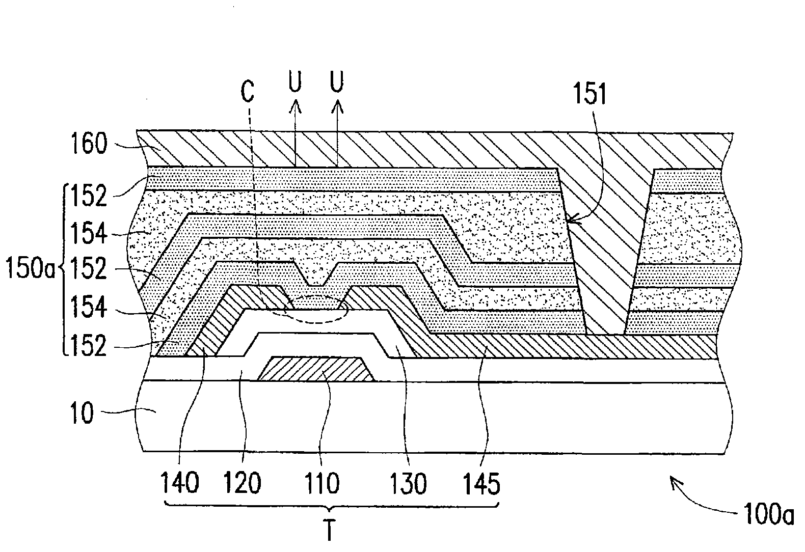
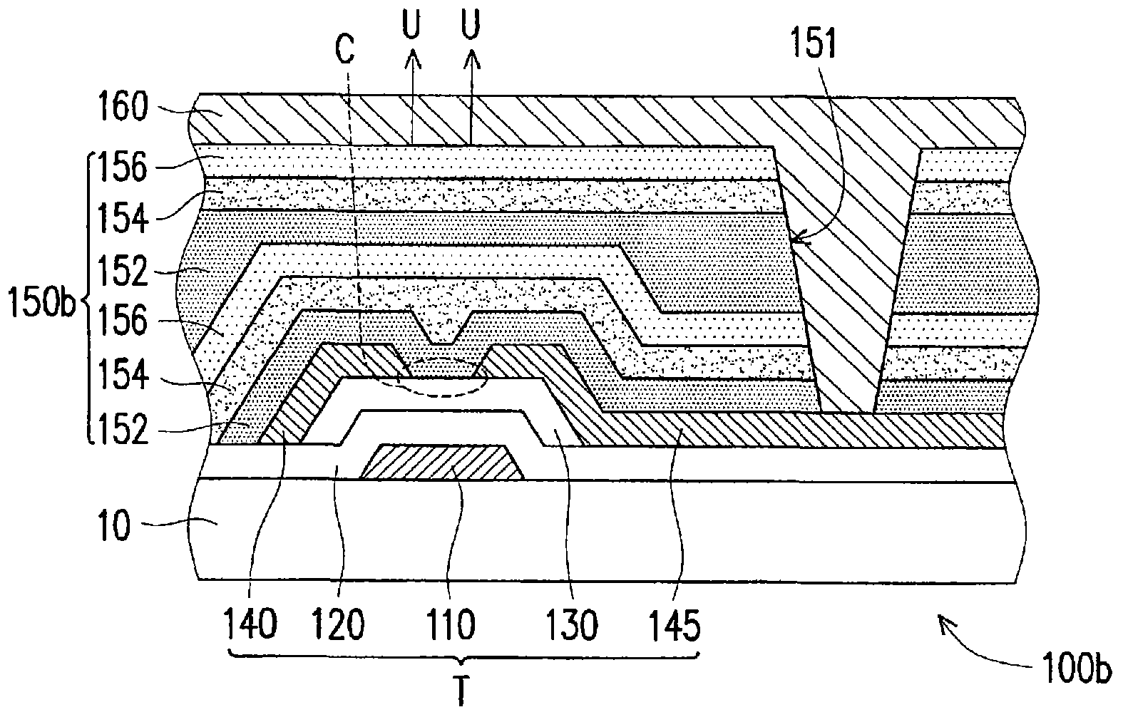
[0031] figure 1 It is a schematic cross-sectional view of a semiconductor structure according to an embodiment of the present invention. Please refer to figure 1 , in this embodiment, the semiconductor structure 100 a includes a gate 110 , a gate insulating layer 120 , an oxide channel layer 130 , a source 140 , a drain 145 and a dielectric stack 150 a.

[0032] In detail, the gate 110 is disposed on a substrate 10 , wherein the gate 110 may be composed of a metal stack or a single metal layer, and its material is, for example, aluminum, copper...


PUM


Abstract

A semiconductor structure includes a gate, an oxide channel layer, a gate insulating layer, a source, a drain and a dielectric stacked layer. The oxide channel layer is stacked over the gate, with the gate insulting layer disposed therebetween. The source and the drain are disposed on a side of the oxide channel layer and in parallel to each other. A portion of the oxide channel layer is exposed between the source and the drain. The dielectric stacked layer is disposed on the substrate and includes plural of first inorganic dielectric layers with a first refraction index and plural of second inorganic dielectric layers with a second refraction index that are stacked alternately. At least one of the first inorganic dielectric layers directly covers the source, the drain and the portion of the oxide channel layer. The first refraction index is smaller than the second refraction index.

Description

technical field [0001] The present invention relates to a semiconductor structure, and in particular to a semiconductor structure having an oxide channel layer. Background technique [0002] Taking the currently most popular liquid crystal display as an example, it is mainly composed of a thin film transistor array substrate, a color filter substrate, and a liquid crystal layer sandwiched between them. On the existing known thin film transistor array substrates, amorphous silicon (a-Si) thin film transistors or low temperature polysilicon thin film transistors are often used as switching elements of each sub-pixel. In recent years, studies have pointed out that oxide semiconductor thin film transistors have higher carrier mobility than amorphous silicon thin film transistors, and oxide semiconductor thin film transistors have higher mobility than low-temperature polysilicon thin film transistors. , it has the advantages of large-area and low-cost production. Therefore, oxi...

Claims


Application Information

Patent Timeline
Patent Type & Authority Applications(China)
IPC IPC(8): H01L29/786H01L29/06
CPCH01L29/78633H01L29/7869H01L29/78609
Inventor 余宗玮舒芳安蔡耀州林冠峄
Owner E INK HLDG INC
Why Eureka
Try Eureka